AT89STK-06 Demo Board ..............................................................................................
Section 1 Introduction ........................................................................................... 1-1 1.1 Features ....................................................................................................1-1 Section 2 Hardware Description ........................................................................... 2-3 2.1 2.2 2.3 2.4 2.5 Block Diagram...........................................................................................2-3 Power Supply .....................
Section 1 Introduction This document describes the board included in the AT89STK-06 Starter Kit dedicated to the T89C51CC01/CC02 and AT89C51CC03 CAN microcontrollers (for T89C51CC02 optionnal adaptor is required). This board is designed to allow an easy evaluation of the product using demonstration software. The AT89STK-06 Starter Kit can be used with the AT89C51AC3, TR89C51AC2, and T89C5115 Flash Microcontrollers with ADC (for T89C5115 optional adapter is required). 1.
Introduction Figure 1-1.
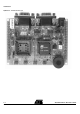
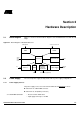
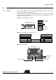
Section 2 Hardware Description 2.1 Block Diagram Figure 2-1 shows a functional block diagram of the AT89STK-06 board, with the I/O usage. Figure 2-1. Block Diagram of AT89STK-06 board CAN Network FLIP, Host, Batch ISP CAN Reset, ISP, INT0, INT1 t°C UART Applicable MCU Sensor 2.2 Power Supply 2.2.
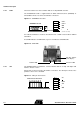
Hardware Description – No specific polarization mandatory Note: There is a diode voltage level between the negative output of the power supply and the “GND”. This could introduce some gap of voltage during measurement and instrumentation. Figure 2-2 . Male JACK Outlet and Wires + - Caution: Do not mount more than one power supply source on AT89STK-06 board.
Hardware Description 2.4 Serial Interfaces 2.4.1 RS-232C All CAN microcontrollers have one on-chip UART peripheral. Only the asynchronous mode is supported by the AT89STK-06 board. The AT89STK-06 board is supplied with a RS-232 driver/receiver. Only one female DB9 connector assumes the RS-232 connections. A full range of configuration can be set with two Rx lines and two Tx lines. Figure 2-4 .
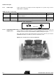
Hardware Description 2.4.2 CAN The microcontroller is a microcontroller with an on-chip full-CAN controller. The AT89STK-06 board is supplied with an Atmel CAN transceiver (ATA6660). A female DB9 connector assumes the CAN bus connections. Figure 2-7 . CAN DB9 Connections CAN DB9 front view 1 2 3 4 5 6 7 8 9 pin 2 CAN-L pin 7 CAN-H pin 3 pin 6 Gnd Gnd pin 5 CAN-SHLD (Can be set to Gnd) If a network termination is needed, JP3 switch inserts a 120Ω resistor between CAN-H and CAN-L.
Hardware Description 2.5 Board Settings The AT89STK-06 board has two types of settings: Jumpers Solder strap Test points Table 2-1, Table 2-2 and Table 2-3 provide an overview of the available settings and test points. 2.5.1 Jumpers Table 2-1.
Hardware Description 2.5.2 Solder straps Solder straps allow to modify the board configuration for specific usage such as T89C51CC02 compatibility. Table 2-2. Table of Solder Strap Reference PCB Name Comments (guidelines) Default SP1 CC02 & C5115 mode For T89C51CC02 usage, allows to redirect the ISP signal to P1.0, for hardware conditions.
2.5.3 Test Points Test points are used to check the internal power supply for AT89STK-06 Board. Table 2-3. Table of Test Points Reference PCB Name Comments (guidelines) TP1 Vref Vref for ADC TP2 Vpot Test point for Potentiometer voltage TP3 Vtemp Test point for Termal resitor voltage TP4 Vcc Test point for Vcc TP5 GND Test point for GND AT89STK-06 Demo Board User Guide 2-9 Rev.
Section 3 Device Programming 3.1 In-System Programming 3.1.1 Manual ISP Mode 3.1.1.1 Board Configuration The on-chip memories and configuration bytes of the AT89C51CC0x parts can be programmed using the ISP mode of the device. To use ISP mode, the board should be configured as follow: POWER switch (SW1) on “ON” position EA jumper should be open (internal code execution only).
Section 4 Appendix A: Board Layout Figure 4-1. Board Components View Diagram J1 AT89STK-06 Demo Board User Guide J2 4-13 Rev.
Appendix B: Bill of Materials Appendix B: Bill of Materials Figure 4-2.
A B C VCC JP1 EA ISP_FLASH /BUZZER ADC_Temp ADC_Pot /EA RX_UART TX_UART /INT0 /INT1 A16 R2 10 K TWI_scl TWI_sda CS_RAM CS_FLASH VAREF P1.[0..7] 5 C5 22 nF C3 100 nF VCC P1.4/AN4/CEX1 P1.5/AN5/CEX2 P1.6/AN6/CEX3 P1.7/AN7/CEX4 EA P3.0/RxD P3.1/TxD P3.2/INT0/ P3.3/INT1/ P3.4/T0 P3.5/T1 U2 RST AT89C51CC03_PLCC44 7 8 9 10 11 12 13 14 15 16 17 AGND DECOUPLING CAPACITOR CLOSE TO THE DEVICE AT89C51CC01/03_PLCC44 P1.7 P1.6 P1.5 P1.4 P3.0 P3.1 P3.2 P3.3 P3.4 P3.5 D P2.[0..
4-16 4339B–CAN–11/04 A B C D P3.[0..7] P1.[0..7] 5 5 P1.0 Vcc_CPU P1.1 Vss P1.2 TWI_sda P1.3 TWI_scl P1.4 /TWI_IT P1.5 /RST P1.6 /EA P1.7 /BP1 P3.0 A16 P3.1 CS_RAM P3.2 Vss P3.3 Xtal2 P3.4 Vss P3.5 Spare0 /WD Spare1 /RD Spare2 P5.0 Spare3 P5.1 Spare4 P5.2 Spare5 P5.3 Spare6 P5.4 Spare7 P5.5 /Buzzer P5.6 Vss P5.
A B C D 1 6 2 7 3 8 4 9 5 VCC 5 DCD DSR Rx_PC RTS Tx_PC CTS DTR C24 100 nF AT6660 SUB-D9 FEMALE RS232 P2 RS232 I/O P4.1 P4.0 1 RxDC TxDC 2 2 4 1 3 5 RXD TXD 8 2 7 6 C1+ C1C2+ C2- R1IN R2IN T1OUT T2OUT V- V+ R1OUT R2OUT T1IN T2IN 1 3 4 5 13 8 14 7 R10 120 4 6 2 12 9 11 10 V- V+ R1OUT R2OUT T1IN T2IN 6 2 12 9 11 10 C23 0.1 µF Vcc Vcc Vcc 1 1.2 K R14 3 Vcc Rx_MCU 9 2 VCC U6C 74HC125/SO 8 74HC125/SO 3 D6 LED PWR RED RS-Rx 1.
A B C 5 3 2 1 XTAL2_44 XTAL2_52 Clock Circuit /RST_UART RST /RST SW5 PUSHBUTTON RESET Reset Circuit CONNECTOR JACK PWR Power J4 1 3 + 4 Vcc R19 1 U10A 4 "Solder Strap" 3 CD74HC14D VOUT 2 Title C29 100 nF R20 AGND C30 4.7 µF R17 1.2 K 1 74HC14D XTAL2 3 C32 100 nF 2 Date: Size A4 Monday, May 24, 2004 Document Number CC0x_demob/POWER 0 1 VCC TP4 Sheet GND TP5 PWR VCC VIN VCC D8 LED PWR RED 1 U9 MC78M05CDT VPOWER 2 Charge U10B 4 C28 4.
Appendix D: Default Configuration Appendix D: Default Configuration Table 1. Default Configuration Reference Name Function State SP1 CC02 mode For T89C51CC02/T89C5115 usage, allow to redirect the ISP signal to P1.0, for hardware conditions.
Appendix E: References/Acronyms Appendix E: References/Acronyms 4.1 References AT89C51CC03, T89C51CC02, T89C51CC01, T89C5115, AT89C51AC3, T89C51AC2 Product Datasheets* 4.
Atmel Headquarters Atmel Operations Corporate Headquarters Memory 2325 Orchard Parkway San Jose, CA 95131 TEL 1(408) 441-0311 FAX 1(408) 487-2600 Europe Atmel Sarl Route des Arsenaux 41 Case Postale 80 CH-1705 Fribourg Switzerland TEL (41) 26-426-5555 FAX (41) 26-426-5500 Asia Room 1219 Chinachem Golden Plaza 77 Mody Road Tsimhatsui East Kowloon Hong Kong TEL (852) 2721-9778 FAX (852) 2722-1369 Japan 9F, Tonetsu Shinkawa Bldg.