
Datasheet
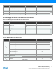
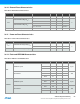
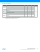
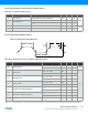
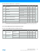
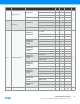
Table Of Contents
- Features
- 1. Ordering Information
- 2. Typical Applications
- 3. Pinout and Block Diagram
- 4. Overview
- 5. Resources
- 6. Capacitive Touch Sensing
- 7. CPU
- 8. Memories
- 9. EDMA – Enhanced DMA Controller
- 10. Event System
- 11. System Clock and Clock options
- 11.1 Features
- 11.2 Overview
- 11.3 Clock Sources
- 11.3.1 32kHz Ultra Low Power Internal Oscillator
- 11.3.2 32.768kHz Calibrated Internal Oscillator
- 11.3.3 32.768kHz Crystal Oscillator
- 11.3.4 0.4 - 16MHz Crystal Oscillator
- 11.3.5 8MHz Calibrated Internal Oscillator
- 11.3.6 32MHz Run-time Calibrated Internal Oscillator
- 11.3.7 External Clock Sources
- 11.3.8 PLL with 1x-31x Multiplication Factor
- 12. Power Management and Sleep Modes
- 13. System Control and Reset
- 14. WDT – Watchdog Timer
- 15. Interrupts and Programmable Multilevel Interrupt Controller
- 16. I/O Ports
- 17. Timer Counter Type 4 and 5
- 18. WeX – Waveform Extension
- 19. Hi-Res – High Resolution Extension
- 20. Fault Extension
- 21. RTC – 16-bit Real-Time Counter
- 22. TWI – Two-Wire Interface
- 23. SPI – Serial Peripheral Interface
- 24. USART
- 25. IRCOM – IR Communication Module
- 26. XCL – XMEGA Custom Logic Module
- 27. CRC – Cyclic Redundancy Check Generator
- 28. ADC – 12-bit Analog to Digital Converter
- 29. DAC – Digital to Analog Converter
- 30. AC – Analog Comparator
- 31. Programming and Debugging
- 32. Pinout and Pin Functions
- 33. Peripheral Module Address Map
- 34. Instruction Set Summary
- 35. Packaging Information
- 36. Electrical Characteristics
- 36.1 Absolute Maximum Ratings
- 36.2 General Operating Ratings
- 36.3 Current Consumption
- 36.4 Wake-up Time from Sleep Modes
- 36.5 I/O Pin Characteristics
- 36.6 ADC Characteristics
- 36.7 DAC Characteristics
- 36.8 Analog Comparator Characteristics
- 36.9 Bandgap and Internal 1.0V Reference Characteristics
- 36.10 External Reset Characteristics
- 36.11 Power-on Reset Characteristics
- 36.12 Flash and EEPROM Characteristics
- 36.13 Clock and Oscillator Characteristics
- 36.13.1 Calibrated 32.768kHz Internal Oscillator Characteristics
- 36.13.2 Calibrated 8MHz Internal Oscillator Characteristics
- 36.13.3 Calibrated and Tunable 32MHz Internal Oscillator Characteristics
- 36.13.4 32 kHz Internal ULP Oscillator Characteristics
- 36.13.5 Internal Phase Locked Loop (PLL) Characteristics
- 36.13.6 External Clock Characteristics
- 36.13.7 External 16MHz Crystal Oscillator and XOSC Characteristics
- 36.13.8 External 32.768kHz Crystal Oscillator and TOSC Characteristics
- 36.14 SPI Characteristics
- 36.15 Two-Wire Interface Characteristics
- 37. Typical Characteristics
- 37.1 Current Consumption
- 37.2 I/O Pin Characteristics
- 37.3 ADC Characteristics
- 37.4 DAC Characteristics
- 37.5 AC Characteristics
- 37.6 Internal 1.0V Reference Characteristics
- 37.7 BOD Characteristics
- 37.8 External Reset Characteristics
- 37.9 Power-on Reset Characteristics
- 37.10 Oscillator Characteristics
- 37.11 Two-wire Interface Characteristics
- 37.12 PDI Characteristics
- 38. Errata – ATxmega32E5 / ATxmega16E5 / ATxmega8E5
- 39. Revision History
- Table of Contents
86
XMEGA E5 [DATASHEET]
Atmel-8153J–AVR-ATxmega8E5-ATxmega16E5-ATxmega32E5_Datasheet–11/2014
Table 36-26. External Clock with Prescaler
(1)
for System Clock
Notes: 1. System Clock Prescalers must be set so that maximum CPU clock frequency for device is not exceeded.
2. The maximum frequency vs. supply voltage is linear between 1.6V and 2.7V, and the same applies for all other parameters with supply voltage conditions.
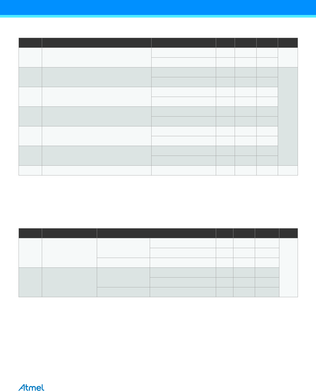
36.13.7 External 16MHz Crystal Oscillator and XOSC Characteristics
Table 36-27. External 16MHz Crystal Oscillator and XOSC Characteristics
Symbol Parameter Condition Min. Typ. Max. Units
1/t
CK
Clock Frequency
(2)
V
CC
= 1.6 - 1.8V 0 90
MHz
V
CC
= 2.7 - 3.6V 0 142
t
CK
Clock Period
V
CC
= 1.6 - 1.8V 11
ns
V
CC
= 2.7 - 3.6V 7
t
CH
Clock High Time
V
CC
= 1.6 - 1.8V 4.5
V
CC
= 2.7 - 3.6V 2.4
t
CL
Clock Low Time
V
CC
= 1.6 - 1.8V 4.5
V
CC
= 2.7 - 3.6V 2.4
t
CR
Rise Time (for maximum frequency)
V
CC
= 1.6 - 1.8V 1.5
V
CC
= 2.7 - 3.6V 1.0
t
CF
Fall Time (for maximum frequency)
V
CC
= 1.6 - 1.8V 1.5
V
CC
= 2.7 - 3.6V 1.0
t
CK
Change in period from one clock cycle to the next 10 %
Symbol Parameter Condition Min. Typ. Max. Units
Cycle to cycle jitter
XOSCPWR=0
FRQRANGE=0 <10
ns
FRQRANGE=1, 2, or 3 <1
XOSCPWR=1 <1
Long term jitter
XOSCPWR=0
FRQRANGE=0 <6
FRQRANGE=1, 2, or 3 <0.5
XOSCPWR=1 <0.5