
Datasheet
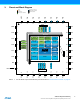
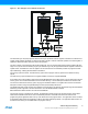
Table Of Contents
- Features
- 1. Ordering Information
- 2. Typical Applications
- 3. Pinout and Block Diagram
- 4. Overview
- 5. Resources
- 6. Capacitive Touch Sensing
- 7. CPU
- 8. Memories
- 9. EDMA – Enhanced DMA Controller
- 10. Event System
- 11. System Clock and Clock options
- 11.1 Features
- 11.2 Overview
- 11.3 Clock Sources
- 11.3.1 32kHz Ultra Low Power Internal Oscillator
- 11.3.2 32.768kHz Calibrated Internal Oscillator
- 11.3.3 32.768kHz Crystal Oscillator
- 11.3.4 0.4 - 16MHz Crystal Oscillator
- 11.3.5 8MHz Calibrated Internal Oscillator
- 11.3.6 32MHz Run-time Calibrated Internal Oscillator
- 11.3.7 External Clock Sources
- 11.3.8 PLL with 1x-31x Multiplication Factor
- 12. Power Management and Sleep Modes
- 13. System Control and Reset
- 14. WDT – Watchdog Timer
- 15. Interrupts and Programmable Multilevel Interrupt Controller
- 16. I/O Ports
- 17. Timer Counter Type 4 and 5
- 18. WeX – Waveform Extension
- 19. Hi-Res – High Resolution Extension
- 20. Fault Extension
- 21. RTC – 16-bit Real-Time Counter
- 22. TWI – Two-Wire Interface
- 23. SPI – Serial Peripheral Interface
- 24. USART
- 25. IRCOM – IR Communication Module
- 26. XCL – XMEGA Custom Logic Module
- 27. CRC – Cyclic Redundancy Check Generator
- 28. ADC – 12-bit Analog to Digital Converter
- 29. DAC – Digital to Analog Converter
- 30. AC – Analog Comparator
- 31. Programming and Debugging
- 32. Pinout and Pin Functions
- 33. Peripheral Module Address Map
- 34. Instruction Set Summary
- 35. Packaging Information
- 36. Electrical Characteristics
- 36.1 Absolute Maximum Ratings
- 36.2 General Operating Ratings
- 36.3 Current Consumption
- 36.4 Wake-up Time from Sleep Modes
- 36.5 I/O Pin Characteristics
- 36.6 ADC Characteristics
- 36.7 DAC Characteristics
- 36.8 Analog Comparator Characteristics
- 36.9 Bandgap and Internal 1.0V Reference Characteristics
- 36.10 External Reset Characteristics
- 36.11 Power-on Reset Characteristics
- 36.12 Flash and EEPROM Characteristics
- 36.13 Clock and Oscillator Characteristics
- 36.13.1 Calibrated 32.768kHz Internal Oscillator Characteristics
- 36.13.2 Calibrated 8MHz Internal Oscillator Characteristics
- 36.13.3 Calibrated and Tunable 32MHz Internal Oscillator Characteristics
- 36.13.4 32 kHz Internal ULP Oscillator Characteristics
- 36.13.5 Internal Phase Locked Loop (PLL) Characteristics
- 36.13.6 External Clock Characteristics
- 36.13.7 External 16MHz Crystal Oscillator and XOSC Characteristics
- 36.13.8 External 32.768kHz Crystal Oscillator and TOSC Characteristics
- 36.14 SPI Characteristics
- 36.15 Two-Wire Interface Characteristics
- 37. Typical Characteristics
- 37.1 Current Consumption
- 37.2 I/O Pin Characteristics
- 37.3 ADC Characteristics
- 37.4 DAC Characteristics
- 37.5 AC Characteristics
- 37.6 Internal 1.0V Reference Characteristics
- 37.7 BOD Characteristics
- 37.8 External Reset Characteristics
- 37.9 Power-on Reset Characteristics
- 37.10 Oscillator Characteristics
- 37.11 Two-wire Interface Characteristics
- 37.12 PDI Characteristics
- 38. Errata – ATxmega32E5 / ATxmega16E5 / ATxmega8E5
- 39. Revision History
- Table of Contents
8
XMEGA E5 [DATASHEET]
Atmel-8153J–AVR-ATxmega8E5-ATxmega16E5-ATxmega32E5_Datasheet–11/2014
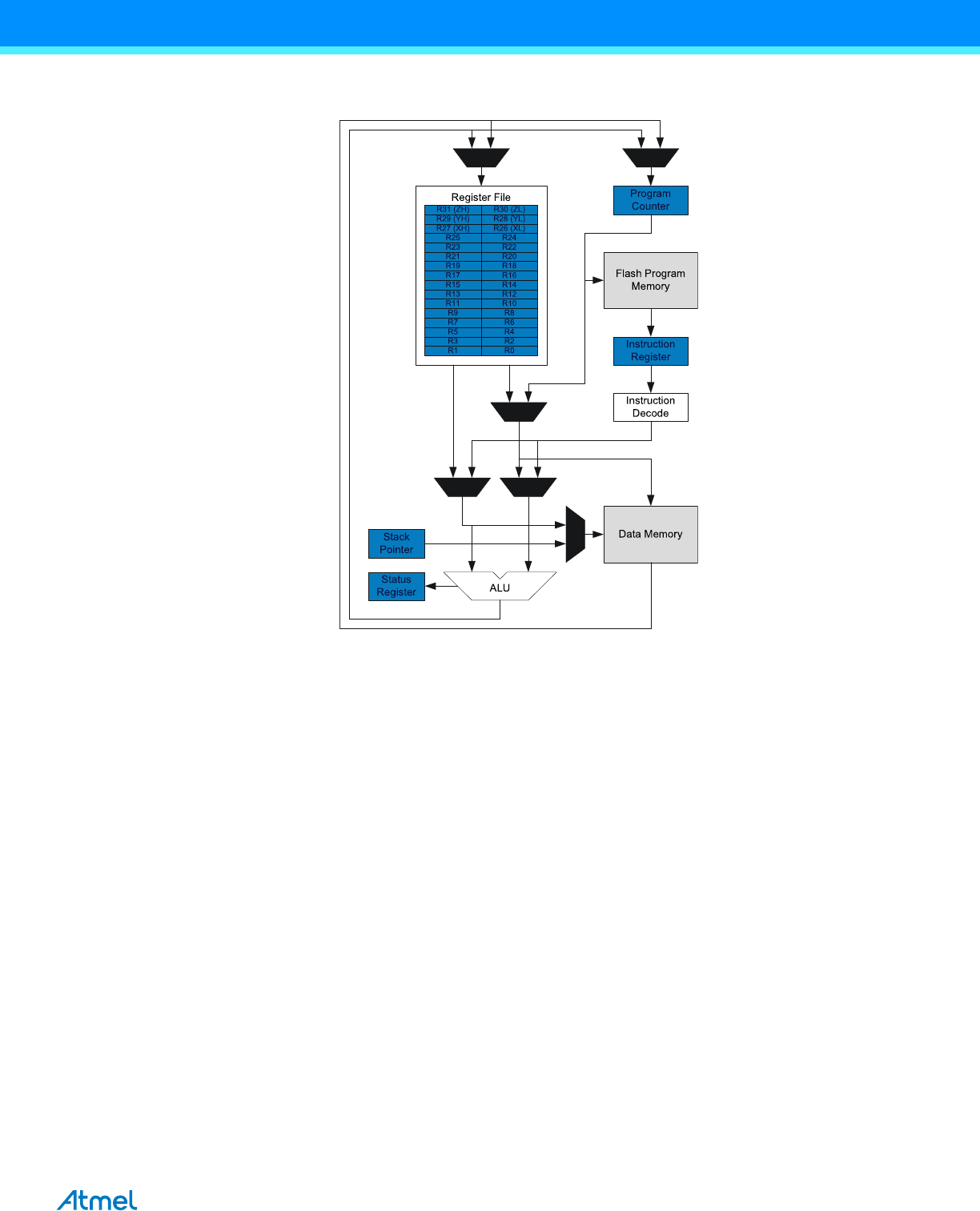
Figure 7-1. Block Diagram of the AVR CPU Architecture
The arithmetic logic unit (ALU) supports arithmetic and logic operations between registers or between a constant and a
register. Single-register operations can also be executed in the ALU. After an arithmetic operation, the status register is
updated to reflect information about the result of the operation.
The ALU is directly connected to the fast-access register file. The 32 x 8-bit general purpose working registers all have
single clock cycle access time allowing single-cycle arithmetic logic unit (ALU) operation between registers or between a
register and an immediate. Six of the 32 registers can be used as three 16-bit address pointers for program and data
space addressing, enabling efficient address calculations.
The memory spaces are linear. The data memory space and the program memory space are two different memory
spaces.
The data memory space is divided into I/O registers, SRAM, and memory mapped EEPROM.
All I/O status and control registers reside in the lowest 4KB addresses of the data memory. This is referred to as the I/O
memory space. The lowest 64 addresses can be accessed directly, or as the data space locations from 0x00 to 0x3F.
The rest is the extended I/O memory space, ranging from 0x0040 to 0x0FFF. I/O registers here must be accessed as
data space locations using load (LD/LDS/LDD) and store (ST/STS/STD) instructions.
The SRAM holds data. Code execution from SRAM is not supported. It can easily be accessed through the five different
addressing modes supported in the AVR architecture. The first SRAM address is 0x2000.
Data addresses 0x1000 to 0x1FFF are reserved for EEPROM.
The program memory is divided in two sections, the application program section and the boot program section. Both
sections have dedicated lock bits for write and read/write protection. The SPM instruction that is used for self-
programming of the application flash memory must reside in the boot program section. The application section contains
an application table section with separate lock bits for write and read/write protection. The application table section can
be used for save storing of nonvolatile data in the program memory.