
Datasheet
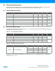
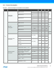
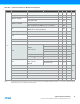
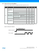
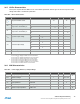
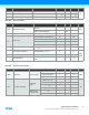
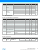
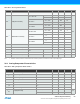
Table Of Contents
- Features
- 1. Ordering Information
- 2. Typical Applications
- 3. Pinout and Block Diagram
- 4. Overview
- 5. Resources
- 6. Capacitive Touch Sensing
- 7. CPU
- 8. Memories
- 9. EDMA – Enhanced DMA Controller
- 10. Event System
- 11. System Clock and Clock options
- 11.1 Features
- 11.2 Overview
- 11.3 Clock Sources
- 11.3.1 32kHz Ultra Low Power Internal Oscillator
- 11.3.2 32.768kHz Calibrated Internal Oscillator
- 11.3.3 32.768kHz Crystal Oscillator
- 11.3.4 0.4 - 16MHz Crystal Oscillator
- 11.3.5 8MHz Calibrated Internal Oscillator
- 11.3.6 32MHz Run-time Calibrated Internal Oscillator
- 11.3.7 External Clock Sources
- 11.3.8 PLL with 1x-31x Multiplication Factor
- 12. Power Management and Sleep Modes
- 13. System Control and Reset
- 14. WDT – Watchdog Timer
- 15. Interrupts and Programmable Multilevel Interrupt Controller
- 16. I/O Ports
- 17. Timer Counter Type 4 and 5
- 18. WeX – Waveform Extension
- 19. Hi-Res – High Resolution Extension
- 20. Fault Extension
- 21. RTC – 16-bit Real-Time Counter
- 22. TWI – Two-Wire Interface
- 23. SPI – Serial Peripheral Interface
- 24. USART
- 25. IRCOM – IR Communication Module
- 26. XCL – XMEGA Custom Logic Module
- 27. CRC – Cyclic Redundancy Check Generator
- 28. ADC – 12-bit Analog to Digital Converter
- 29. DAC – Digital to Analog Converter
- 30. AC – Analog Comparator
- 31. Programming and Debugging
- 32. Pinout and Pin Functions
- 33. Peripheral Module Address Map
- 34. Instruction Set Summary
- 35. Packaging Information
- 36. Electrical Characteristics
- 36.1 Absolute Maximum Ratings
- 36.2 General Operating Ratings
- 36.3 Current Consumption
- 36.4 Wake-up Time from Sleep Modes
- 36.5 I/O Pin Characteristics
- 36.6 ADC Characteristics
- 36.7 DAC Characteristics
- 36.8 Analog Comparator Characteristics
- 36.9 Bandgap and Internal 1.0V Reference Characteristics
- 36.10 External Reset Characteristics
- 36.11 Power-on Reset Characteristics
- 36.12 Flash and EEPROM Characteristics
- 36.13 Clock and Oscillator Characteristics
- 36.13.1 Calibrated 32.768kHz Internal Oscillator Characteristics
- 36.13.2 Calibrated 8MHz Internal Oscillator Characteristics
- 36.13.3 Calibrated and Tunable 32MHz Internal Oscillator Characteristics
- 36.13.4 32 kHz Internal ULP Oscillator Characteristics
- 36.13.5 Internal Phase Locked Loop (PLL) Characteristics
- 36.13.6 External Clock Characteristics
- 36.13.7 External 16MHz Crystal Oscillator and XOSC Characteristics
- 36.13.8 External 32.768kHz Crystal Oscillator and TOSC Characteristics
- 36.14 SPI Characteristics
- 36.15 Two-Wire Interface Characteristics
- 37. Typical Characteristics
- 37.1 Current Consumption
- 37.2 I/O Pin Characteristics
- 37.3 ADC Characteristics
- 37.4 DAC Characteristics
- 37.5 AC Characteristics
- 37.6 Internal 1.0V Reference Characteristics
- 37.7 BOD Characteristics
- 37.8 External Reset Characteristics
- 37.9 Power-on Reset Characteristics
- 37.10 Oscillator Characteristics
- 37.11 Two-wire Interface Characteristics
- 37.12 PDI Characteristics
- 38. Errata – ATxmega32E5 / ATxmega16E5 / ATxmega8E5
- 39. Revision History
- Table of Contents
76
XMEGA E5 [DATASHEET]
Atmel-8153J–AVR-ATxmega8E5-ATxmega16E5-ATxmega32E5_Datasheet–11/2014
36.5 I/O Pin Characteristics
The I/O pins complies with the JEDEC LVTTL and LVCMOS specification and the high- and low-level input and output
voltage limits reflect or exceed this specification.
Table 36-6. I/O Pin Characteristics
Notes: 1. The sum of all I
OH
for PA[7:5] on PORTA must not exceed 100mA.
The sum of all I
OH
for PA[4:0] on PORTA must not exceed 200mA.
The sum of all I
OH
for PORTD and PORTR must not exceed 100mA.
The sum of all I
OH
for PORTC and PDI must not exceed 100mA.
2. The sum of all I
OL
for PA[7:5] on PORTA must not exceed 100mA.
The sum of all I
OL
for PA[4:0] on PORTA must not exceed 100mA.
The sum of all I
OL
for PORTD and PORTR must not exceed 100mA.
The sum of all I
OL
for PORTC PDI must not exceed 100mA.
36.6 ADC Characteristics
Table 36-7. Power Supply, Reference, and Input Range
Symbol Parameter Condition Min. Typ. Max. Units
I
OH
(1)
/
I
OL
(2)
I/O pin source/sink current -15 15 mA
V
IH
High level input voltage,
except XTAL1 and RESET pin
V
CC
= 2.4 - 3.6V 0.7*V
CC
V
CC
+0.5
V
V
CC
= 1.6 - 2.4V 0.8*V
CC
V
CC
+0.5
V
IL
Low level input voltage,
except XTAL1 and RESET pin
V
CC
= 2.4 - 3.6V -0.5 0.3*V
CC
V
CC
= 1.6 - 2.4V -0.5 0.2*V
CC
V
OH
High level output voltage
V
CC
= 3.3V I
OH
= -4mA 2.6 3.1
V
CC
= 3.0V I
OH
= -3mA 2.1 2.7
V
CC
= 1.8V I
OH
= -1mA 1.4 1.7
V
OL
Low level output voltage
V
CC
= 3.3V I
OL
= 8mA 0.20 0.76
V
CC
= 3.0V I
OL
= 5mA 0.15 0.64
V
CC
= 1.8V I
OL
= 3mA 0.10 0.46
I
IN
Input leakage current T = 25°C <0.01 1.0 µA
R
P
Pull/buss keeper resistor 27 k
Symbol Parameter Condition Min. Typ. Max. Units
AV
CC
Analog supply voltage V
CC
- 0.3 V
CC
+ 0.3
V
V
REF
Reference voltage 1 AV
CC
- 0.6
R
in
Input resistance Switched 4.5 k
C
in
Input capacitance Switched 5 pF
R
AREF
Reference input resistance (leakage only) >10 M
C
AREF
Reference input capacitance Static load 7 pF