
Datasheet
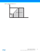
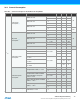
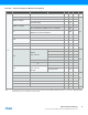
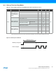
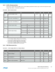
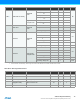
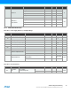
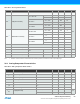
Table Of Contents
- Features
- 1. Ordering Information
- 2. Typical Applications
- 3. Pinout and Block Diagram
- 4. Overview
- 5. Resources
- 6. Capacitive Touch Sensing
- 7. CPU
- 8. Memories
- 9. EDMA – Enhanced DMA Controller
- 10. Event System
- 11. System Clock and Clock options
- 11.1 Features
- 11.2 Overview
- 11.3 Clock Sources
- 11.3.1 32kHz Ultra Low Power Internal Oscillator
- 11.3.2 32.768kHz Calibrated Internal Oscillator
- 11.3.3 32.768kHz Crystal Oscillator
- 11.3.4 0.4 - 16MHz Crystal Oscillator
- 11.3.5 8MHz Calibrated Internal Oscillator
- 11.3.6 32MHz Run-time Calibrated Internal Oscillator
- 11.3.7 External Clock Sources
- 11.3.8 PLL with 1x-31x Multiplication Factor
- 12. Power Management and Sleep Modes
- 13. System Control and Reset
- 14. WDT – Watchdog Timer
- 15. Interrupts and Programmable Multilevel Interrupt Controller
- 16. I/O Ports
- 17. Timer Counter Type 4 and 5
- 18. WeX – Waveform Extension
- 19. Hi-Res – High Resolution Extension
- 20. Fault Extension
- 21. RTC – 16-bit Real-Time Counter
- 22. TWI – Two-Wire Interface
- 23. SPI – Serial Peripheral Interface
- 24. USART
- 25. IRCOM – IR Communication Module
- 26. XCL – XMEGA Custom Logic Module
- 27. CRC – Cyclic Redundancy Check Generator
- 28. ADC – 12-bit Analog to Digital Converter
- 29. DAC – Digital to Analog Converter
- 30. AC – Analog Comparator
- 31. Programming and Debugging
- 32. Pinout and Pin Functions
- 33. Peripheral Module Address Map
- 34. Instruction Set Summary
- 35. Packaging Information
- 36. Electrical Characteristics
- 36.1 Absolute Maximum Ratings
- 36.2 General Operating Ratings
- 36.3 Current Consumption
- 36.4 Wake-up Time from Sleep Modes
- 36.5 I/O Pin Characteristics
- 36.6 ADC Characteristics
- 36.7 DAC Characteristics
- 36.8 Analog Comparator Characteristics
- 36.9 Bandgap and Internal 1.0V Reference Characteristics
- 36.10 External Reset Characteristics
- 36.11 Power-on Reset Characteristics
- 36.12 Flash and EEPROM Characteristics
- 36.13 Clock and Oscillator Characteristics
- 36.13.1 Calibrated 32.768kHz Internal Oscillator Characteristics
- 36.13.2 Calibrated 8MHz Internal Oscillator Characteristics
- 36.13.3 Calibrated and Tunable 32MHz Internal Oscillator Characteristics
- 36.13.4 32 kHz Internal ULP Oscillator Characteristics
- 36.13.5 Internal Phase Locked Loop (PLL) Characteristics
- 36.13.6 External Clock Characteristics
- 36.13.7 External 16MHz Crystal Oscillator and XOSC Characteristics
- 36.13.8 External 32.768kHz Crystal Oscillator and TOSC Characteristics
- 36.14 SPI Characteristics
- 36.15 Two-Wire Interface Characteristics
- 37. Typical Characteristics
- 37.1 Current Consumption
- 37.2 I/O Pin Characteristics
- 37.3 ADC Characteristics
- 37.4 DAC Characteristics
- 37.5 AC Characteristics
- 37.6 Internal 1.0V Reference Characteristics
- 37.7 BOD Characteristics
- 37.8 External Reset Characteristics
- 37.9 Power-on Reset Characteristics
- 37.10 Oscillator Characteristics
- 37.11 Two-wire Interface Characteristics
- 37.12 PDI Characteristics
- 38. Errata – ATxmega32E5 / ATxmega16E5 / ATxmega8E5
- 39. Revision History
- Table of Contents
71
XMEGA E5 [DATASHEET]
Atmel-8153J–AVR-ATxmega8E5-ATxmega16E5-ATxmega32E5_Datasheet–11/2014
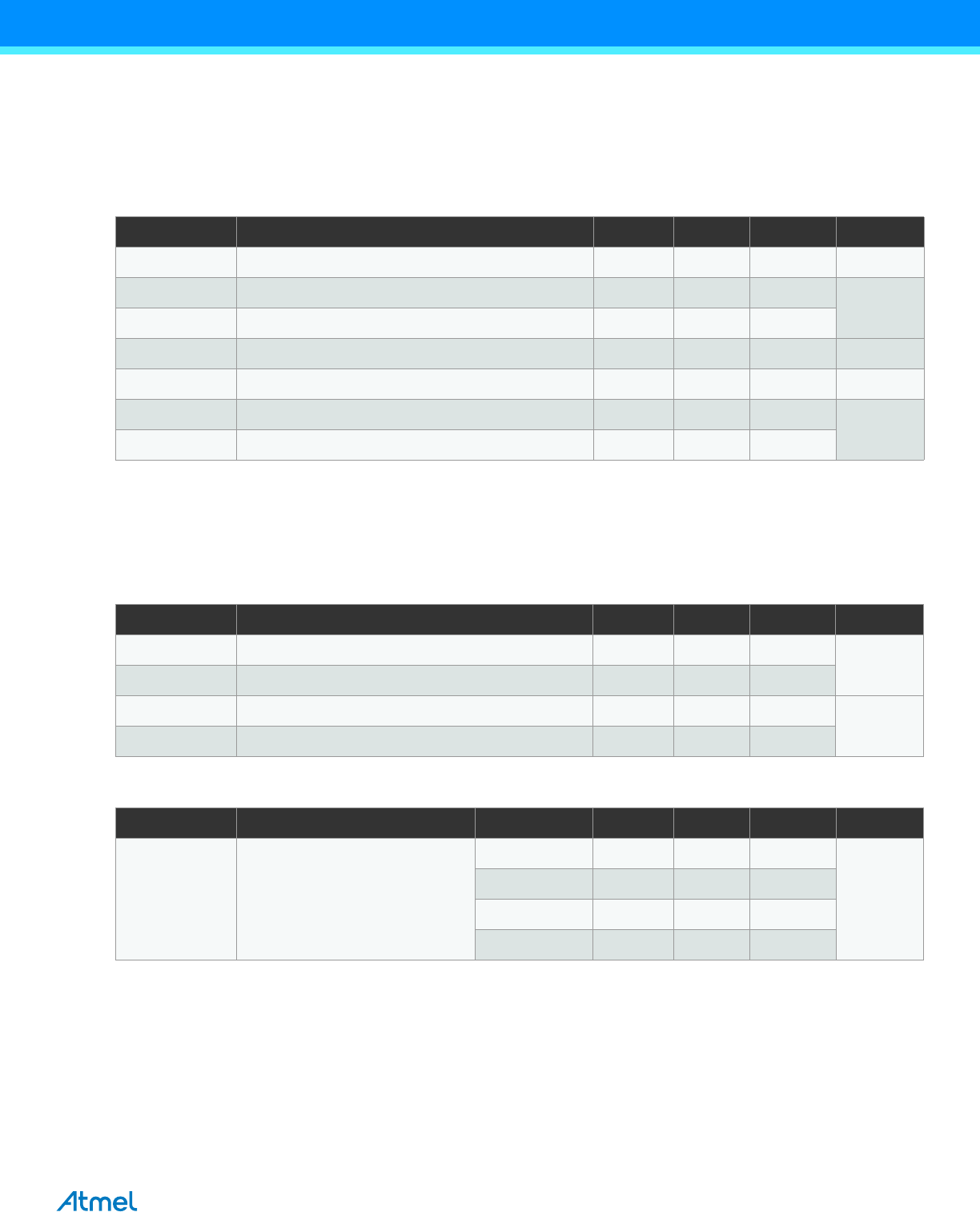
36. Electrical Characteristics
All typical values are measured at T = 25°C unless other temperature condition is given. All minimum and maximum
values are valid across operating temperature and voltage unless other conditions are given.
36.1 Absolute Maximum Ratings
36.2 General Operating Ratings
The device must operate within the ratings listed in Table 36-1 in order for all other electrical characteristics and typical
characteristics of the device to be valid.
Table 36-1. General Operating Conditions
Table 36-2. Operating Voltage and Frequency
The maximum CPU clock frequency depends on V
CC
. As shown in Figure 36-1 the frequency vs. V
CC
curve is linear
between 1.8V < V
CC
<2.7V.
Symbol Parameter Min. Typ. Max. Units
V
CC
Power supply voltage -0.3 4 V
I
VCC
Current into a V
CC
pin 200
mA
I
GND
Current out of a Gnd pin 200
V
PIN
Pin voltage with respect to Gnd and V
CC
-0.5 V
CC
+0.5 V
I
PIN
I/O pin sink/source current -25 25 mA
T
A
Storage temperature -65 150
°C
T
j
Junction temperature 150
Symbol Parameter Min. Typ. Max. Units
V
CC
Power supply voltage 1.6 3.6
V
AV
CC
Analog supply voltage 1.6 3.6
T
A
Temperature range -40 85
°C
T
j
Junction temperature -40 105
Symbol Parameter Condition Min. Typ. Max. Units
Clk
CPU
CPU clock frequency
V
CC
= 1.6V 0 12
MHz
V
CC
= 1.8V 0 12
V
CC
= 2.7V 0 32
V
CC
= 3.6V 0 32