
Datasheet
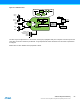
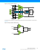
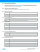
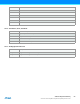
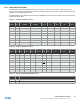
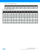
Table Of Contents
- Features
- 1. Ordering Information
- 2. Typical Applications
- 3. Pinout and Block Diagram
- 4. Overview
- 5. Resources
- 6. Capacitive Touch Sensing
- 7. CPU
- 8. Memories
- 9. EDMA – Enhanced DMA Controller
- 10. Event System
- 11. System Clock and Clock options
- 11.1 Features
- 11.2 Overview
- 11.3 Clock Sources
- 11.3.1 32kHz Ultra Low Power Internal Oscillator
- 11.3.2 32.768kHz Calibrated Internal Oscillator
- 11.3.3 32.768kHz Crystal Oscillator
- 11.3.4 0.4 - 16MHz Crystal Oscillator
- 11.3.5 8MHz Calibrated Internal Oscillator
- 11.3.6 32MHz Run-time Calibrated Internal Oscillator
- 11.3.7 External Clock Sources
- 11.3.8 PLL with 1x-31x Multiplication Factor
- 12. Power Management and Sleep Modes
- 13. System Control and Reset
- 14. WDT – Watchdog Timer
- 15. Interrupts and Programmable Multilevel Interrupt Controller
- 16. I/O Ports
- 17. Timer Counter Type 4 and 5
- 18. WeX – Waveform Extension
- 19. Hi-Res – High Resolution Extension
- 20. Fault Extension
- 21. RTC – 16-bit Real-Time Counter
- 22. TWI – Two-Wire Interface
- 23. SPI – Serial Peripheral Interface
- 24. USART
- 25. IRCOM – IR Communication Module
- 26. XCL – XMEGA Custom Logic Module
- 27. CRC – Cyclic Redundancy Check Generator
- 28. ADC – 12-bit Analog to Digital Converter
- 29. DAC – Digital to Analog Converter
- 30. AC – Analog Comparator
- 31. Programming and Debugging
- 32. Pinout and Pin Functions
- 33. Peripheral Module Address Map
- 34. Instruction Set Summary
- 35. Packaging Information
- 36. Electrical Characteristics
- 36.1 Absolute Maximum Ratings
- 36.2 General Operating Ratings
- 36.3 Current Consumption
- 36.4 Wake-up Time from Sleep Modes
- 36.5 I/O Pin Characteristics
- 36.6 ADC Characteristics
- 36.7 DAC Characteristics
- 36.8 Analog Comparator Characteristics
- 36.9 Bandgap and Internal 1.0V Reference Characteristics
- 36.10 External Reset Characteristics
- 36.11 Power-on Reset Characteristics
- 36.12 Flash and EEPROM Characteristics
- 36.13 Clock and Oscillator Characteristics
- 36.13.1 Calibrated 32.768kHz Internal Oscillator Characteristics
- 36.13.2 Calibrated 8MHz Internal Oscillator Characteristics
- 36.13.3 Calibrated and Tunable 32MHz Internal Oscillator Characteristics
- 36.13.4 32 kHz Internal ULP Oscillator Characteristics
- 36.13.5 Internal Phase Locked Loop (PLL) Characteristics
- 36.13.6 External Clock Characteristics
- 36.13.7 External 16MHz Crystal Oscillator and XOSC Characteristics
- 36.13.8 External 32.768kHz Crystal Oscillator and TOSC Characteristics
- 36.14 SPI Characteristics
- 36.15 Two-Wire Interface Characteristics
- 37. Typical Characteristics
- 37.1 Current Consumption
- 37.2 I/O Pin Characteristics
- 37.3 ADC Characteristics
- 37.4 DAC Characteristics
- 37.5 AC Characteristics
- 37.6 Internal 1.0V Reference Characteristics
- 37.7 BOD Characteristics
- 37.8 External Reset Characteristics
- 37.9 Power-on Reset Characteristics
- 37.10 Oscillator Characteristics
- 37.11 Two-wire Interface Characteristics
- 37.12 PDI Characteristics
- 38. Errata – ATxmega32E5 / ATxmega16E5 / ATxmega8E5
- 39. Revision History
- Table of Contents
59
XMEGA E5 [DATASHEET]
Atmel-8153J–AVR-ATxmega8E5-ATxmega16E5-ATxmega32E5_Datasheet–11/2014
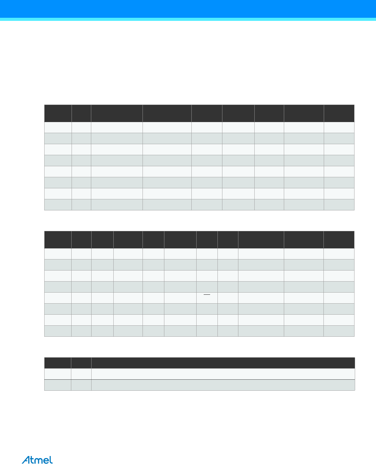
32.2 Alternate Pin Functions
The tables below show the primary/default function for each pin on a port in the first column, the pin number in the
second column, and then all alternate pin functions in the remaining columns. The head row shows what peripheral that
enable and use the alternate pin functions.
For better flexibility, some alternate functions also have selectable pin locations for their functions, this is noted under the
first table where this apply.
Table 32-1. PORT A – Alternate Functions
Table 32-2. PORT C – Alternate Functions
Table 32-3. Debug – Program and Debug Functions
PORT A Pin#
ADCA POS/
GAINPOS
ADCA NEG/
GAINNEG
DACA
ACA
POS
ACA
NEG
ACA
OUT
REFA
PA0 6 ADC 0 ADC 0 AC0 AC0 AREF
PA1 5 ADC 1 ADC 1 AC1 AC1
PA2 4 ADC 2 ADC 2 DAC0 AC2
PA3 3 ADC 3 ADC 3 DAC1 AC3 AC3
PA4 2 ADC 4 ADC 4 AC4
PA5 31 ADC 5 ADC 5 AC5 AC5
PA6 30 ADC 6 ADC 6 AC6 AC1OUT
PA7 29 ADC 7 ADC 7 AC7 AC0OUT
PORT C Pin # TCC4 WEXC TCC5 USARTC0 SPIC TWI
XCL
(LUT)
EXTCLK AC OUT
PC0 16 OC4A OC4ALS SDA IN1/OUT0
PC1 15 OC4B OC4AHS XCK0 SCL IN2
PC2 14 OC4C OC4BLS RXD0 IN0
PC3 13 OC4D OC4BHS TXD0 IN3
PC4 12 OC4A OC4CLS OC5A SS IN1/OUT0 EXTCLK
PC5 11 OC4B OC4CHS OC5B XCK0 SCK IN2
PC6 10 OC4C OC4DLS RXD0 MISO IN0 AC1OUT
PC7 9 OC4D OC4DHS TXD0 MOSI IN3 AC0OUT
DEBUG Pin # PROG
RESET 8 PDI CLOCK
PDI 7 PDI DATA