
Datasheet
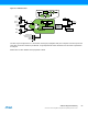
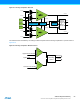
Table Of Contents
- Features
- 1. Ordering Information
- 2. Typical Applications
- 3. Pinout and Block Diagram
- 4. Overview
- 5. Resources
- 6. Capacitive Touch Sensing
- 7. CPU
- 8. Memories
- 9. EDMA – Enhanced DMA Controller
- 10. Event System
- 11. System Clock and Clock options
- 11.1 Features
- 11.2 Overview
- 11.3 Clock Sources
- 11.3.1 32kHz Ultra Low Power Internal Oscillator
- 11.3.2 32.768kHz Calibrated Internal Oscillator
- 11.3.3 32.768kHz Crystal Oscillator
- 11.3.4 0.4 - 16MHz Crystal Oscillator
- 11.3.5 8MHz Calibrated Internal Oscillator
- 11.3.6 32MHz Run-time Calibrated Internal Oscillator
- 11.3.7 External Clock Sources
- 11.3.8 PLL with 1x-31x Multiplication Factor
- 12. Power Management and Sleep Modes
- 13. System Control and Reset
- 14. WDT – Watchdog Timer
- 15. Interrupts and Programmable Multilevel Interrupt Controller
- 16. I/O Ports
- 17. Timer Counter Type 4 and 5
- 18. WeX – Waveform Extension
- 19. Hi-Res – High Resolution Extension
- 20. Fault Extension
- 21. RTC – 16-bit Real-Time Counter
- 22. TWI – Two-Wire Interface
- 23. SPI – Serial Peripheral Interface
- 24. USART
- 25. IRCOM – IR Communication Module
- 26. XCL – XMEGA Custom Logic Module
- 27. CRC – Cyclic Redundancy Check Generator
- 28. ADC – 12-bit Analog to Digital Converter
- 29. DAC – Digital to Analog Converter
- 30. AC – Analog Comparator
- 31. Programming and Debugging
- 32. Pinout and Pin Functions
- 33. Peripheral Module Address Map
- 34. Instruction Set Summary
- 35. Packaging Information
- 36. Electrical Characteristics
- 36.1 Absolute Maximum Ratings
- 36.2 General Operating Ratings
- 36.3 Current Consumption
- 36.4 Wake-up Time from Sleep Modes
- 36.5 I/O Pin Characteristics
- 36.6 ADC Characteristics
- 36.7 DAC Characteristics
- 36.8 Analog Comparator Characteristics
- 36.9 Bandgap and Internal 1.0V Reference Characteristics
- 36.10 External Reset Characteristics
- 36.11 Power-on Reset Characteristics
- 36.12 Flash and EEPROM Characteristics
- 36.13 Clock and Oscillator Characteristics
- 36.13.1 Calibrated 32.768kHz Internal Oscillator Characteristics
- 36.13.2 Calibrated 8MHz Internal Oscillator Characteristics
- 36.13.3 Calibrated and Tunable 32MHz Internal Oscillator Characteristics
- 36.13.4 32 kHz Internal ULP Oscillator Characteristics
- 36.13.5 Internal Phase Locked Loop (PLL) Characteristics
- 36.13.6 External Clock Characteristics
- 36.13.7 External 16MHz Crystal Oscillator and XOSC Characteristics
- 36.13.8 External 32.768kHz Crystal Oscillator and TOSC Characteristics
- 36.14 SPI Characteristics
- 36.15 Two-Wire Interface Characteristics
- 37. Typical Characteristics
- 37.1 Current Consumption
- 37.2 I/O Pin Characteristics
- 37.3 ADC Characteristics
- 37.4 DAC Characteristics
- 37.5 AC Characteristics
- 37.6 Internal 1.0V Reference Characteristics
- 37.7 BOD Characteristics
- 37.8 External Reset Characteristics
- 37.9 Power-on Reset Characteristics
- 37.10 Oscillator Characteristics
- 37.11 Two-wire Interface Characteristics
- 37.12 PDI Characteristics
- 38. Errata – ATxmega32E5 / ATxmega16E5 / ATxmega8E5
- 39. Revision History
- Table of Contents

56
XMEGA E5 [DATASHEET]
Atmel-8153J–AVR-ATxmega8E5-ATxmega16E5-ATxmega32E5_Datasheet–11/2014
31. Programming and Debugging
31.1 Features
Programming
External programming through PDI interface
Minimal protocol overhead for fast operation
Built-in error detection and handling for reliable operation
Boot loader support for programming through any communication interface
Debugging
Nonintrusive, real-time, on-chip debug system
No software or hardware resources required from device except pin connection
Program flow control
Go, Stop, Reset, Step Into, Step Over, Step Out, Run-to-Cursor
Unlimited number of user program breakpoints
Unlimited number of user data breakpoints, break on:
Data location read, write, or both read and write
Data location content equal or not equal to a value
Data location content is greater or smaller than a value
Data location content is within or outside a range
No limitation on device clock frequency
Program and Debug Interface (PDI)
Two-pin interface for external programming and debugging
Uses the Reset pin and a dedicated pin
No I/O pins required during programming or debugging
31.2 Overview
The Program and Debug Interface (PDI) is an Atmel proprietary interface for external programming and on-chip
debugging of a device. The PDI supports fast programming of nonvolatile memory (NVM) spaces; flash, EEPOM, fuses,
lock bits, and the user signature row.
Debug is supported through an on-chip debug system that offers nonintrusive, real-time debug. It does not require any
software or hardware resources except for the device pin connection. Using the Atmel tool chain, it offers complete
program flow control and support for an unlimited number of program and complex data breakpoints. Application debug
can be done from a C or other high-level language source code level, as well as from an assembler and disassemble
level.
Programming and debugging can be done through the PDI physical layer. This is a two-pin interface that uses the Reset
pin for the clock input (PDI_CLK) and one other dedicated pin for data input and output (PDI_DATA). Any external
programmer or on-chip debugger/emulator can be directly connected to this interface.