
Datasheet
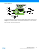
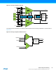
Table Of Contents
- Features
- 1. Ordering Information
- 2. Typical Applications
- 3. Pinout and Block Diagram
- 4. Overview
- 5. Resources
- 6. Capacitive Touch Sensing
- 7. CPU
- 8. Memories
- 9. EDMA – Enhanced DMA Controller
- 10. Event System
- 11. System Clock and Clock options
- 11.1 Features
- 11.2 Overview
- 11.3 Clock Sources
- 11.3.1 32kHz Ultra Low Power Internal Oscillator
- 11.3.2 32.768kHz Calibrated Internal Oscillator
- 11.3.3 32.768kHz Crystal Oscillator
- 11.3.4 0.4 - 16MHz Crystal Oscillator
- 11.3.5 8MHz Calibrated Internal Oscillator
- 11.3.6 32MHz Run-time Calibrated Internal Oscillator
- 11.3.7 External Clock Sources
- 11.3.8 PLL with 1x-31x Multiplication Factor
- 12. Power Management and Sleep Modes
- 13. System Control and Reset
- 14. WDT – Watchdog Timer
- 15. Interrupts and Programmable Multilevel Interrupt Controller
- 16. I/O Ports
- 17. Timer Counter Type 4 and 5
- 18. WeX – Waveform Extension
- 19. Hi-Res – High Resolution Extension
- 20. Fault Extension
- 21. RTC – 16-bit Real-Time Counter
- 22. TWI – Two-Wire Interface
- 23. SPI – Serial Peripheral Interface
- 24. USART
- 25. IRCOM – IR Communication Module
- 26. XCL – XMEGA Custom Logic Module
- 27. CRC – Cyclic Redundancy Check Generator
- 28. ADC – 12-bit Analog to Digital Converter
- 29. DAC – Digital to Analog Converter
- 30. AC – Analog Comparator
- 31. Programming and Debugging
- 32. Pinout and Pin Functions
- 33. Peripheral Module Address Map
- 34. Instruction Set Summary
- 35. Packaging Information
- 36. Electrical Characteristics
- 36.1 Absolute Maximum Ratings
- 36.2 General Operating Ratings
- 36.3 Current Consumption
- 36.4 Wake-up Time from Sleep Modes
- 36.5 I/O Pin Characteristics
- 36.6 ADC Characteristics
- 36.7 DAC Characteristics
- 36.8 Analog Comparator Characteristics
- 36.9 Bandgap and Internal 1.0V Reference Characteristics
- 36.10 External Reset Characteristics
- 36.11 Power-on Reset Characteristics
- 36.12 Flash and EEPROM Characteristics
- 36.13 Clock and Oscillator Characteristics
- 36.13.1 Calibrated 32.768kHz Internal Oscillator Characteristics
- 36.13.2 Calibrated 8MHz Internal Oscillator Characteristics
- 36.13.3 Calibrated and Tunable 32MHz Internal Oscillator Characteristics
- 36.13.4 32 kHz Internal ULP Oscillator Characteristics
- 36.13.5 Internal Phase Locked Loop (PLL) Characteristics
- 36.13.6 External Clock Characteristics
- 36.13.7 External 16MHz Crystal Oscillator and XOSC Characteristics
- 36.13.8 External 32.768kHz Crystal Oscillator and TOSC Characteristics
- 36.14 SPI Characteristics
- 36.15 Two-Wire Interface Characteristics
- 37. Typical Characteristics
- 37.1 Current Consumption
- 37.2 I/O Pin Characteristics
- 37.3 ADC Characteristics
- 37.4 DAC Characteristics
- 37.5 AC Characteristics
- 37.6 Internal 1.0V Reference Characteristics
- 37.7 BOD Characteristics
- 37.8 External Reset Characteristics
- 37.9 Power-on Reset Characteristics
- 37.10 Oscillator Characteristics
- 37.11 Two-wire Interface Characteristics
- 37.12 PDI Characteristics
- 38. Errata – ATxmega32E5 / ATxmega16E5 / ATxmega8E5
- 39. Revision History
- Table of Contents

51
XMEGA E5 [DATASHEET]
Atmel-8153J–AVR-ATxmega8E5-ATxmega16E5-ATxmega32E5_Datasheet–11/2014
28. ADC – 12-bit Analog to Digital Converter
28.1 Features
12-bit resolution
Up to 300 thousand samples per second
Down to 2.3μs conversion time with 8-bit resolution
Down to 3.35μs conversion time with 12-bit resolution
Differential and single-ended input
Up to 16 single-ended inputs
16x8 differential inputs with optional gain
Built-in differential gain stage
1/2x, 1x, 2x, 4x, 8x, 16x, 32x, and 64x gain options
Single, continuous and scan conversion options
Four internal inputs
Internal temperature sensor
DAC output
AV
CC
voltage divided by 10
1.1V bandgap voltage
Internal and external reference options
Compare function for accurate monitoring of user defined thresholds
Offset and gain correction
Averaging
Over-sampling and decimation
Optional event triggered conversion for accurate timing
Optional interrupt/event on compare result
Optional EDMA transfer of conversion results
28.2 Overview
The ADC converts analog signals to digital values. The ADC has 12-bit resolution and is capable of converting up to 300
thousand samples per second (ksps). The input selection is flexible, and both single-ended and differential
measurements can be done. For differential measurements, an optional gain stage is available to increase the dynamic
range. In addition, several internal signal inputs are available. The ADC can provide both signed and unsigned results.
The ADC measurements can either be started by application software or an incoming event from another peripheral in
the device. The ADC measurements can be started with predictable timing, and without software intervention. It is
possible to use EDMA to move ADC results directly to memory or peripherals when conversions are done.
Both internal and external reference voltages can be used. An integrated temperature sensor is available for use with the
ADC. The output from the DAC, AV
CC
/10, and the bandgap voltage can also be measured by the ADC.
The ADC has a compare function for accurate monitoring of user defined thresholds with minimum software intervention
required.
When operation in noisy conditions, the average feature can be enabled to increase the ADC resolution. Up to 1024
samples can be averaged, enabling up to 16-bit resolution results. In the same way, using the over-sampling and
decimation mode, the ADC resolution is increased up to 16-bits, which results in up to 4-bit extra lsb resolution. The ADC
includes various calibration options. In addition to standard production calibration, the user can enable the offset and
gain correction to improve the absolute ADC accuracy.