
Datasheet
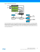

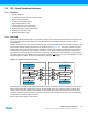
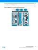
Table Of Contents
- Features
- 1. Ordering Information
- 2. Typical Applications
- 3. Pinout and Block Diagram
- 4. Overview
- 5. Resources
- 6. Capacitive Touch Sensing
- 7. CPU
- 8. Memories
- 9. EDMA – Enhanced DMA Controller
- 10. Event System
- 11. System Clock and Clock options
- 11.1 Features
- 11.2 Overview
- 11.3 Clock Sources
- 11.3.1 32kHz Ultra Low Power Internal Oscillator
- 11.3.2 32.768kHz Calibrated Internal Oscillator
- 11.3.3 32.768kHz Crystal Oscillator
- 11.3.4 0.4 - 16MHz Crystal Oscillator
- 11.3.5 8MHz Calibrated Internal Oscillator
- 11.3.6 32MHz Run-time Calibrated Internal Oscillator
- 11.3.7 External Clock Sources
- 11.3.8 PLL with 1x-31x Multiplication Factor
- 12. Power Management and Sleep Modes
- 13. System Control and Reset
- 14. WDT – Watchdog Timer
- 15. Interrupts and Programmable Multilevel Interrupt Controller
- 16. I/O Ports
- 17. Timer Counter Type 4 and 5
- 18. WeX – Waveform Extension
- 19. Hi-Res – High Resolution Extension
- 20. Fault Extension
- 21. RTC – 16-bit Real-Time Counter
- 22. TWI – Two-Wire Interface
- 23. SPI – Serial Peripheral Interface
- 24. USART
- 25. IRCOM – IR Communication Module
- 26. XCL – XMEGA Custom Logic Module
- 27. CRC – Cyclic Redundancy Check Generator
- 28. ADC – 12-bit Analog to Digital Converter
- 29. DAC – Digital to Analog Converter
- 30. AC – Analog Comparator
- 31. Programming and Debugging
- 32. Pinout and Pin Functions
- 33. Peripheral Module Address Map
- 34. Instruction Set Summary
- 35. Packaging Information
- 36. Electrical Characteristics
- 36.1 Absolute Maximum Ratings
- 36.2 General Operating Ratings
- 36.3 Current Consumption
- 36.4 Wake-up Time from Sleep Modes
- 36.5 I/O Pin Characteristics
- 36.6 ADC Characteristics
- 36.7 DAC Characteristics
- 36.8 Analog Comparator Characteristics
- 36.9 Bandgap and Internal 1.0V Reference Characteristics
- 36.10 External Reset Characteristics
- 36.11 Power-on Reset Characteristics
- 36.12 Flash and EEPROM Characteristics
- 36.13 Clock and Oscillator Characteristics
- 36.13.1 Calibrated 32.768kHz Internal Oscillator Characteristics
- 36.13.2 Calibrated 8MHz Internal Oscillator Characteristics
- 36.13.3 Calibrated and Tunable 32MHz Internal Oscillator Characteristics
- 36.13.4 32 kHz Internal ULP Oscillator Characteristics
- 36.13.5 Internal Phase Locked Loop (PLL) Characteristics
- 36.13.6 External Clock Characteristics
- 36.13.7 External 16MHz Crystal Oscillator and XOSC Characteristics
- 36.13.8 External 32.768kHz Crystal Oscillator and TOSC Characteristics
- 36.14 SPI Characteristics
- 36.15 Two-Wire Interface Characteristics
- 37. Typical Characteristics
- 37.1 Current Consumption
- 37.2 I/O Pin Characteristics
- 37.3 ADC Characteristics
- 37.4 DAC Characteristics
- 37.5 AC Characteristics
- 37.6 Internal 1.0V Reference Characteristics
- 37.7 BOD Characteristics
- 37.8 External Reset Characteristics
- 37.9 Power-on Reset Characteristics
- 37.10 Oscillator Characteristics
- 37.11 Two-wire Interface Characteristics
- 37.12 PDI Characteristics
- 38. Errata – ATxmega32E5 / ATxmega16E5 / ATxmega8E5
- 39. Revision History
- Table of Contents
44
XMEGA E5 [DATASHEET]
Atmel-8153J–AVR-ATxmega8E5-ATxmega16E5-ATxmega32E5_Datasheet–11/2014
23. SPI – Serial Peripheral Interface
23.1 Features
One SPI peripheral
Full-duplex, three-wire synchronous data transfer
Master or slave operation
lsb first or msb first data transfer
Eight programmable bit rates
Interrupt flag at the end of transmission
Write collision flag to indicate data collision
Wake up from idle sleep mode
Double speed master mode
23.2 Overview
The Serial Peripheral Interface (SPI) is a high-speed, full duplex, synchronous data transfer interface using three or four
pins. It allows fast communication between an AVR XMEGA device and peripheral devices or between several
microcontrollers.
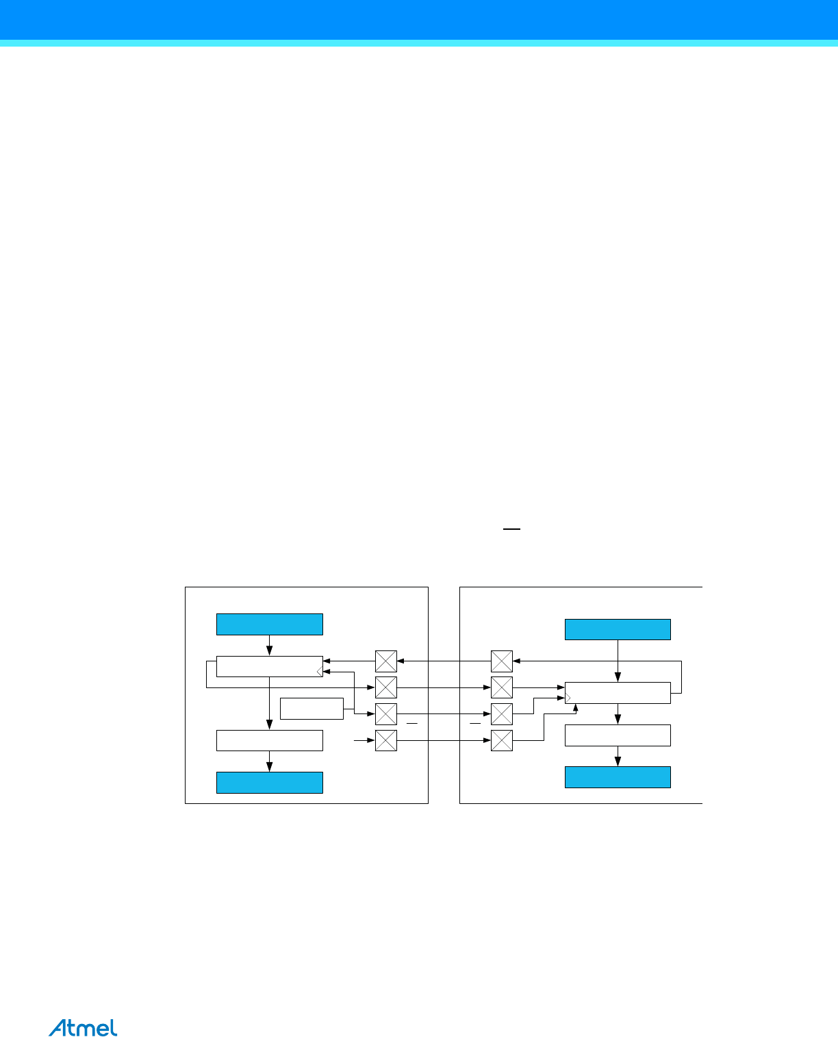
A device connected to the bus must act as a master or slave. The master initiates and controls all data transactions. The
interconnection between master and slave devices with SPI is shown in Figure 23-1. The system consists of two shift
registers and a clock generator. The SPI master initiates the communication by pulling the slave select (SS) signal low
for the desired slave. Master and slave prepare the data to be sent in their respective shift registers, and the master
generates the required clock pulses on the SCK line to interchange data. Data are always shifted from master to slave on
the master output, slave input (MOSI) line, and from slave to master on the master input, slave output (MISO) line. After
each data packet, the master can synchronize the slave by pulling the SS
line high.
Figure 23-1. SPI Master-slave Interconnection
By default, the SPI module is single buffered and transmit direction and double buffered in the receive direction. A byte
written to the transmit data register will be copied to the shift register when a full character has been received. When
receiving data, a received character must be read from the transmit data register before the third character has been
completely shifted in to avoid losing data. Optionally, buffer modes can be enabled. When used, one buffer is available
for transmitter and a double buffer for reception.
PORTC has one SPI. Notation of this is SPIC.
8-bit Shift Register
msb
Transmit Data Register
(DATA)
Receive Buffer Register
Receive Data Register
(DATA)
MOSI lsb
MISO
SCK
SS
SLAVE
8-bit Shift Register
msb
Transmit Data Register
(DATA)
Receive Buffer Register
Receive Data Register
(DATA)
MOSI
lsb MISO
SCK
SS
MASTER
SPI CLOCK
GENERATOR