
Datasheet
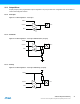
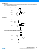
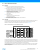

Table Of Contents
- Features
- 1. Ordering Information
- 2. Typical Applications
- 3. Pinout and Block Diagram
- 4. Overview
- 5. Resources
- 6. Capacitive Touch Sensing
- 7. CPU
- 8. Memories
- 9. EDMA – Enhanced DMA Controller
- 10. Event System
- 11. System Clock and Clock options
- 11.1 Features
- 11.2 Overview
- 11.3 Clock Sources
- 11.3.1 32kHz Ultra Low Power Internal Oscillator
- 11.3.2 32.768kHz Calibrated Internal Oscillator
- 11.3.3 32.768kHz Crystal Oscillator
- 11.3.4 0.4 - 16MHz Crystal Oscillator
- 11.3.5 8MHz Calibrated Internal Oscillator
- 11.3.6 32MHz Run-time Calibrated Internal Oscillator
- 11.3.7 External Clock Sources
- 11.3.8 PLL with 1x-31x Multiplication Factor
- 12. Power Management and Sleep Modes
- 13. System Control and Reset
- 14. WDT – Watchdog Timer
- 15. Interrupts and Programmable Multilevel Interrupt Controller
- 16. I/O Ports
- 17. Timer Counter Type 4 and 5
- 18. WeX – Waveform Extension
- 19. Hi-Res – High Resolution Extension
- 20. Fault Extension
- 21. RTC – 16-bit Real-Time Counter
- 22. TWI – Two-Wire Interface
- 23. SPI – Serial Peripheral Interface
- 24. USART
- 25. IRCOM – IR Communication Module
- 26. XCL – XMEGA Custom Logic Module
- 27. CRC – Cyclic Redundancy Check Generator
- 28. ADC – 12-bit Analog to Digital Converter
- 29. DAC – Digital to Analog Converter
- 30. AC – Analog Comparator
- 31. Programming and Debugging
- 32. Pinout and Pin Functions
- 33. Peripheral Module Address Map
- 34. Instruction Set Summary
- 35. Packaging Information
- 36. Electrical Characteristics
- 36.1 Absolute Maximum Ratings
- 36.2 General Operating Ratings
- 36.3 Current Consumption
- 36.4 Wake-up Time from Sleep Modes
- 36.5 I/O Pin Characteristics
- 36.6 ADC Characteristics
- 36.7 DAC Characteristics
- 36.8 Analog Comparator Characteristics
- 36.9 Bandgap and Internal 1.0V Reference Characteristics
- 36.10 External Reset Characteristics
- 36.11 Power-on Reset Characteristics
- 36.12 Flash and EEPROM Characteristics
- 36.13 Clock and Oscillator Characteristics
- 36.13.1 Calibrated 32.768kHz Internal Oscillator Characteristics
- 36.13.2 Calibrated 8MHz Internal Oscillator Characteristics
- 36.13.3 Calibrated and Tunable 32MHz Internal Oscillator Characteristics
- 36.13.4 32 kHz Internal ULP Oscillator Characteristics
- 36.13.5 Internal Phase Locked Loop (PLL) Characteristics
- 36.13.6 External Clock Characteristics
- 36.13.7 External 16MHz Crystal Oscillator and XOSC Characteristics
- 36.13.8 External 32.768kHz Crystal Oscillator and TOSC Characteristics
- 36.14 SPI Characteristics
- 36.15 Two-Wire Interface Characteristics
- 37. Typical Characteristics
- 37.1 Current Consumption
- 37.2 I/O Pin Characteristics
- 37.3 ADC Characteristics
- 37.4 DAC Characteristics
- 37.5 AC Characteristics
- 37.6 Internal 1.0V Reference Characteristics
- 37.7 BOD Characteristics
- 37.8 External Reset Characteristics
- 37.9 Power-on Reset Characteristics
- 37.10 Oscillator Characteristics
- 37.11 Two-wire Interface Characteristics
- 37.12 PDI Characteristics
- 38. Errata – ATxmega32E5 / ATxmega16E5 / ATxmega8E5
- 39. Revision History
- Table of Contents
36
XMEGA E5 [DATASHEET]
Atmel-8153J–AVR-ATxmega8E5-ATxmega16E5-ATxmega32E5_Datasheet–11/2014
18. WeX – Waveform Extension
18.1 Features
Module for more customized and advanced waveform generation
Optimized for various type of motor, ballast, and power stage control
Output matrix for timer/counter waveform output distribution
Configurable distribution of compare channel output across port pins
Redistribution of dead-time insertion resource between TC4 and TC5
Four dead-time insertion (DTI) units, each with
Complementary high and low side with non overlapping outputs
Separate dead-time setting for high and low side
8-bit resolution
Four swap (SWAP) units
Separate port pair or low high side drivers swap
Double buffered swap feature
Pattern generation creating synchronized bit pattern across the port pins
Double buffered pattern generation
18.2 Overview
The waveform extension (WEX) provides extra functions to the timer/counter in waveform generation (WG) modes. It is
primarily intended for motor control, ballast, LED, H-bridge, power converters, and other types of power control
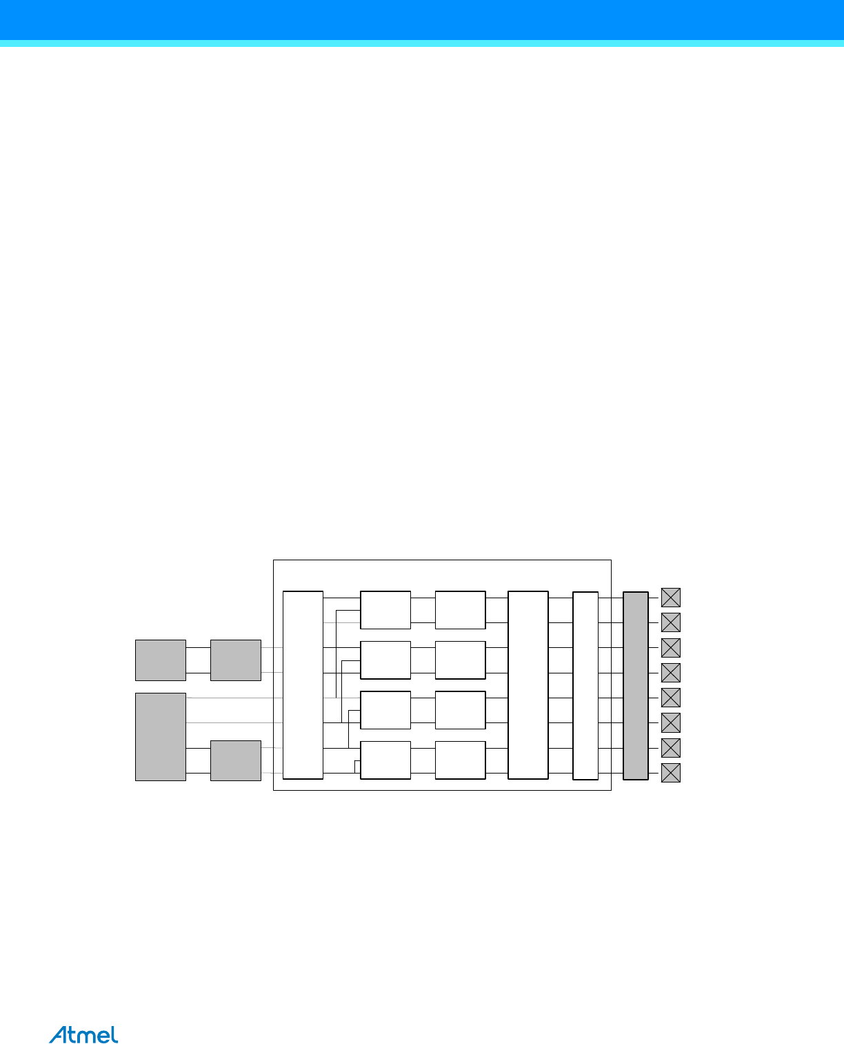
applications. The WEX consist of five independent and successive units, as shown in Figure 18-1.
Figure 18-1. Waveform Extension and Closely Related Peripherals
The output matrix (OTMX) can distribute and route out the waveform outputs from timer/counter 4 and 5 across the port
pins in different configurations, each optimized for different application types. The dead time insertion (DTI) unit splits the
four lower OTMX outputs into a two non-overlapping signals, the non-inverted low side (LS) and inverted high side (HS)
of the waveform output with optional dead-time insertion between LS and HS switching.
The swap (SWAP) unit can swap the LS and HS pin position. This can be used for fast decay motor control. The pattern
generation unit generates synchronized output waveform with constant logic level. This can be used for easy stepper
motor and full bridge control.
SWAP1DTI1
SWAP1DTI1
SWAP1DTI1
SWAP1DTI1
Pattern Generator
Output Matrix
WEX
Px7
Px6
Px5
Px4
Px3
Px2
Px1
Px0
Fault
Unit 5
Fault
Unit 4
T/C4
T/C5
OUTOVDIS
HIRES