
Datasheet
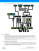
Table Of Contents
- Features
- 1. Ordering Information
- 2. Typical Applications
- 3. Pinout and Block Diagram
- 4. Overview
- 5. Resources
- 6. Capacitive Touch Sensing
- 7. CPU
- 8. Memories
- 9. EDMA – Enhanced DMA Controller
- 10. Event System
- 11. System Clock and Clock options
- 11.1 Features
- 11.2 Overview
- 11.3 Clock Sources
- 11.3.1 32kHz Ultra Low Power Internal Oscillator
- 11.3.2 32.768kHz Calibrated Internal Oscillator
- 11.3.3 32.768kHz Crystal Oscillator
- 11.3.4 0.4 - 16MHz Crystal Oscillator
- 11.3.5 8MHz Calibrated Internal Oscillator
- 11.3.6 32MHz Run-time Calibrated Internal Oscillator
- 11.3.7 External Clock Sources
- 11.3.8 PLL with 1x-31x Multiplication Factor
- 12. Power Management and Sleep Modes
- 13. System Control and Reset
- 14. WDT – Watchdog Timer
- 15. Interrupts and Programmable Multilevel Interrupt Controller
- 16. I/O Ports
- 17. Timer Counter Type 4 and 5
- 18. WeX – Waveform Extension
- 19. Hi-Res – High Resolution Extension
- 20. Fault Extension
- 21. RTC – 16-bit Real-Time Counter
- 22. TWI – Two-Wire Interface
- 23. SPI – Serial Peripheral Interface
- 24. USART
- 25. IRCOM – IR Communication Module
- 26. XCL – XMEGA Custom Logic Module
- 27. CRC – Cyclic Redundancy Check Generator
- 28. ADC – 12-bit Analog to Digital Converter
- 29. DAC – Digital to Analog Converter
- 30. AC – Analog Comparator
- 31. Programming and Debugging
- 32. Pinout and Pin Functions
- 33. Peripheral Module Address Map
- 34. Instruction Set Summary
- 35. Packaging Information
- 36. Electrical Characteristics
- 36.1 Absolute Maximum Ratings
- 36.2 General Operating Ratings
- 36.3 Current Consumption
- 36.4 Wake-up Time from Sleep Modes
- 36.5 I/O Pin Characteristics
- 36.6 ADC Characteristics
- 36.7 DAC Characteristics
- 36.8 Analog Comparator Characteristics
- 36.9 Bandgap and Internal 1.0V Reference Characteristics
- 36.10 External Reset Characteristics
- 36.11 Power-on Reset Characteristics
- 36.12 Flash and EEPROM Characteristics
- 36.13 Clock and Oscillator Characteristics
- 36.13.1 Calibrated 32.768kHz Internal Oscillator Characteristics
- 36.13.2 Calibrated 8MHz Internal Oscillator Characteristics
- 36.13.3 Calibrated and Tunable 32MHz Internal Oscillator Characteristics
- 36.13.4 32 kHz Internal ULP Oscillator Characteristics
- 36.13.5 Internal Phase Locked Loop (PLL) Characteristics
- 36.13.6 External Clock Characteristics
- 36.13.7 External 16MHz Crystal Oscillator and XOSC Characteristics
- 36.13.8 External 32.768kHz Crystal Oscillator and TOSC Characteristics
- 36.14 SPI Characteristics
- 36.15 Two-Wire Interface Characteristics
- 37. Typical Characteristics
- 37.1 Current Consumption
- 37.2 I/O Pin Characteristics
- 37.3 ADC Characteristics
- 37.4 DAC Characteristics
- 37.5 AC Characteristics
- 37.6 Internal 1.0V Reference Characteristics
- 37.7 BOD Characteristics
- 37.8 External Reset Characteristics
- 37.9 Power-on Reset Characteristics
- 37.10 Oscillator Characteristics
- 37.11 Two-wire Interface Characteristics
- 37.12 PDI Characteristics
- 38. Errata – ATxmega32E5 / ATxmega16E5 / ATxmega8E5
- 39. Revision History
- Table of Contents

30
XMEGA E5 [DATASHEET]
Atmel-8153J–AVR-ATxmega8E5-ATxmega16E5-ATxmega32E5_Datasheet–11/2014
16. I/O Ports
16.1 Features
26 general purpose input and output pins with individual configuration
Output driver with configurable driver and pull settings:
Totem-pole
Wired-AND
Wired-OR
Bus-keeper
Inverted I/O
Input with asynchronous sensing with interrupts and events
Sense both edges
Sense rising edges
Sense falling edges
Sense low level
Optional pull-up and pull-down resistor on input and Wired-OR/AND configurations
Optional slew rate control per I/O port
Asynchronous pin change sensing that can wake the device from all sleep modes
One port interrupt with pin masking per I/O port
Efficient and safe access to port pins
Hardware read-modify-write through dedicated toggle/clear/set registers
Configuration of multiple pins in a single operation
Mapping of port registers into bit-accessible I/O memory space
Peripheral clocks output on port pin
Real-time counter clock output to port pin
Event channels can be output on port pin
Remapping of digital peripheral pin functions
Selectable USART and timer/counters input/output pin locations
Selectable Analog Comparator output pin locations
16.2 Overview
One port consists of up to eight pins ranging from pin 0 to 7. Each port pin can be configured as input or output with
configurable driver and pull settings. They also implement asynchronous input sensing with interrupt and events for
selectable pin change conditions.
Asynchronous pin-change sensing means that a pin change can wake the device from all sleep modes, including the
modes where no clocks are running.
All functions are individual and configurable per pin, but several pins can be configured in a single operation. The pins
have hardware read-modify-write (RMW) functionality for safe and correct change of drive value and/or pull resistor
configuration. The direction of one port pin can be changed without unintentionally changing the direction of any other
pin.
The port pin configuration also controls input and output selection of other device functions. It is possible to have both the
peripheral clock and the real-time clock output to a port pin, and available for external use. The same applies to events
from the event system that can be used to synchronize and control external functions. Other digital peripherals, such as
USART, timer/counters, and analog comparator output can be remapped to selectable pin locations in order to optimize
pin-out versus application needs.
The notations of the ports are PORTA, PORTC, PORTD, and PORTR.