
Datasheet
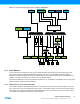
Table Of Contents
- Features
- 1. Ordering Information
- 2. Typical Applications
- 3. Pinout and Block Diagram
- 4. Overview
- 5. Resources
- 6. Capacitive Touch Sensing
- 7. CPU
- 8. Memories
- 9. EDMA – Enhanced DMA Controller
- 10. Event System
- 11. System Clock and Clock options
- 11.1 Features
- 11.2 Overview
- 11.3 Clock Sources
- 11.3.1 32kHz Ultra Low Power Internal Oscillator
- 11.3.2 32.768kHz Calibrated Internal Oscillator
- 11.3.3 32.768kHz Crystal Oscillator
- 11.3.4 0.4 - 16MHz Crystal Oscillator
- 11.3.5 8MHz Calibrated Internal Oscillator
- 11.3.6 32MHz Run-time Calibrated Internal Oscillator
- 11.3.7 External Clock Sources
- 11.3.8 PLL with 1x-31x Multiplication Factor
- 12. Power Management and Sleep Modes
- 13. System Control and Reset
- 14. WDT – Watchdog Timer
- 15. Interrupts and Programmable Multilevel Interrupt Controller
- 16. I/O Ports
- 17. Timer Counter Type 4 and 5
- 18. WeX – Waveform Extension
- 19. Hi-Res – High Resolution Extension
- 20. Fault Extension
- 21. RTC – 16-bit Real-Time Counter
- 22. TWI – Two-Wire Interface
- 23. SPI – Serial Peripheral Interface
- 24. USART
- 25. IRCOM – IR Communication Module
- 26. XCL – XMEGA Custom Logic Module
- 27. CRC – Cyclic Redundancy Check Generator
- 28. ADC – 12-bit Analog to Digital Converter
- 29. DAC – Digital to Analog Converter
- 30. AC – Analog Comparator
- 31. Programming and Debugging
- 32. Pinout and Pin Functions
- 33. Peripheral Module Address Map
- 34. Instruction Set Summary
- 35. Packaging Information
- 36. Electrical Characteristics
- 36.1 Absolute Maximum Ratings
- 36.2 General Operating Ratings
- 36.3 Current Consumption
- 36.4 Wake-up Time from Sleep Modes
- 36.5 I/O Pin Characteristics
- 36.6 ADC Characteristics
- 36.7 DAC Characteristics
- 36.8 Analog Comparator Characteristics
- 36.9 Bandgap and Internal 1.0V Reference Characteristics
- 36.10 External Reset Characteristics
- 36.11 Power-on Reset Characteristics
- 36.12 Flash and EEPROM Characteristics
- 36.13 Clock and Oscillator Characteristics
- 36.13.1 Calibrated 32.768kHz Internal Oscillator Characteristics
- 36.13.2 Calibrated 8MHz Internal Oscillator Characteristics
- 36.13.3 Calibrated and Tunable 32MHz Internal Oscillator Characteristics
- 36.13.4 32 kHz Internal ULP Oscillator Characteristics
- 36.13.5 Internal Phase Locked Loop (PLL) Characteristics
- 36.13.6 External Clock Characteristics
- 36.13.7 External 16MHz Crystal Oscillator and XOSC Characteristics
- 36.13.8 External 32.768kHz Crystal Oscillator and TOSC Characteristics
- 36.14 SPI Characteristics
- 36.15 Two-Wire Interface Characteristics
- 37. Typical Characteristics
- 37.1 Current Consumption
- 37.2 I/O Pin Characteristics
- 37.3 ADC Characteristics
- 37.4 DAC Characteristics
- 37.5 AC Characteristics
- 37.6 Internal 1.0V Reference Characteristics
- 37.7 BOD Characteristics
- 37.8 External Reset Characteristics
- 37.9 Power-on Reset Characteristics
- 37.10 Oscillator Characteristics
- 37.11 Two-wire Interface Characteristics
- 37.12 PDI Characteristics
- 38. Errata – ATxmega32E5 / ATxmega16E5 / ATxmega8E5
- 39. Revision History
- Table of Contents

25
XMEGA E5 [DATASHEET]
Atmel-8153J–AVR-ATxmega8E5-ATxmega16E5-ATxmega32E5_Datasheet–11/2014
13. System Control and Reset
13.1 Features
Reset the microcontroller and set it to initial state when a reset source goes active
Multiple reset sources that cover different situations
Power-on reset
External reset
Watchdog reset
Brownout reset
PDI reset
Software reset
Asynchronous operation
No running system clock in the device is required for reset
Reset status register for reading the reset source from the application code
13.2 Overview
The reset system issues a microcontroller reset and sets the device to its initial state. This is for situations where
operation should not start or continue, such as when the microcontroller operates below its power supply rating. If a reset
source goes active, the device enters and is kept in reset until all reset sources have released their reset. The I/O pins
are immediately tri-stated. The program counter is set to the reset vector location, and all I/O registers are set to their
initial values. The SRAM content is kept. However, if the device accesses the SRAM when a reset occurs, the content of
the accessed location can not be guaranteed.
After reset is released from all reset sources, the default oscillator is started and calibrated before the device starts
running from the reset vector address. By default, this is the lowest program memory address, 0, but it is possible to
move the reset vector to the lowest address in the boot section.
The reset functionality is asynchronous, and so no running system clock is required to reset the device. The software
reset feature makes it possible to issue a controlled system reset from the user software.
The reset status register has individual status flags for each reset source. It is cleared at power-on reset, and shows
which sources have issued a reset since the last power-on.
13.3 Reset Sequence
A reset request from any reset source will immediately reset the device and keep it in reset as long as the request is
active. When all reset requests are released, the device will go through three stages before the device starts running
again:
Reset counter delay
Oscillator startup
Oscillator calibration
If another reset requests occurs during this process, the reset sequence will start over again.
13.4 Reset Sources
13.4.1 Power-on Reset
A power-on reset (POR) is generated by an on-chip detection circuit. The POR is activated when the VCC rises and
reaches the POR threshold voltage (V
POT
), and this will start the reset sequence.
The POR is also activated to power down the device properly when the V
CC falls and drops below the VPOT level. The
V
POT level is higher for falling V
CC
than for rising V
CC
. Consult the datasheet for POR characteristics data.