
Datasheet
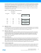
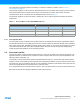
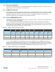
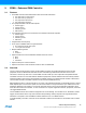

Table Of Contents
- Features
- 1. Ordering Information
- 2. Typical Applications
- 3. Pinout and Block Diagram
- 4. Overview
- 5. Resources
- 6. Capacitive Touch Sensing
- 7. CPU
- 8. Memories
- 9. EDMA – Enhanced DMA Controller
- 10. Event System
- 11. System Clock and Clock options
- 11.1 Features
- 11.2 Overview
- 11.3 Clock Sources
- 11.3.1 32kHz Ultra Low Power Internal Oscillator
- 11.3.2 32.768kHz Calibrated Internal Oscillator
- 11.3.3 32.768kHz Crystal Oscillator
- 11.3.4 0.4 - 16MHz Crystal Oscillator
- 11.3.5 8MHz Calibrated Internal Oscillator
- 11.3.6 32MHz Run-time Calibrated Internal Oscillator
- 11.3.7 External Clock Sources
- 11.3.8 PLL with 1x-31x Multiplication Factor
- 12. Power Management and Sleep Modes
- 13. System Control and Reset
- 14. WDT – Watchdog Timer
- 15. Interrupts and Programmable Multilevel Interrupt Controller
- 16. I/O Ports
- 17. Timer Counter Type 4 and 5
- 18. WeX – Waveform Extension
- 19. Hi-Res – High Resolution Extension
- 20. Fault Extension
- 21. RTC – 16-bit Real-Time Counter
- 22. TWI – Two-Wire Interface
- 23. SPI – Serial Peripheral Interface
- 24. USART
- 25. IRCOM – IR Communication Module
- 26. XCL – XMEGA Custom Logic Module
- 27. CRC – Cyclic Redundancy Check Generator
- 28. ADC – 12-bit Analog to Digital Converter
- 29. DAC – Digital to Analog Converter
- 30. AC – Analog Comparator
- 31. Programming and Debugging
- 32. Pinout and Pin Functions
- 33. Peripheral Module Address Map
- 34. Instruction Set Summary
- 35. Packaging Information
- 36. Electrical Characteristics
- 36.1 Absolute Maximum Ratings
- 36.2 General Operating Ratings
- 36.3 Current Consumption
- 36.4 Wake-up Time from Sleep Modes
- 36.5 I/O Pin Characteristics
- 36.6 ADC Characteristics
- 36.7 DAC Characteristics
- 36.8 Analog Comparator Characteristics
- 36.9 Bandgap and Internal 1.0V Reference Characteristics
- 36.10 External Reset Characteristics
- 36.11 Power-on Reset Characteristics
- 36.12 Flash and EEPROM Characteristics
- 36.13 Clock and Oscillator Characteristics
- 36.13.1 Calibrated 32.768kHz Internal Oscillator Characteristics
- 36.13.2 Calibrated 8MHz Internal Oscillator Characteristics
- 36.13.3 Calibrated and Tunable 32MHz Internal Oscillator Characteristics
- 36.13.4 32 kHz Internal ULP Oscillator Characteristics
- 36.13.5 Internal Phase Locked Loop (PLL) Characteristics
- 36.13.6 External Clock Characteristics
- 36.13.7 External 16MHz Crystal Oscillator and XOSC Characteristics
- 36.13.8 External 32.768kHz Crystal Oscillator and TOSC Characteristics
- 36.14 SPI Characteristics
- 36.15 Two-Wire Interface Characteristics
- 37. Typical Characteristics
- 37.1 Current Consumption
- 37.2 I/O Pin Characteristics
- 37.3 ADC Characteristics
- 37.4 DAC Characteristics
- 37.5 AC Characteristics
- 37.6 Internal 1.0V Reference Characteristics
- 37.7 BOD Characteristics
- 37.8 External Reset Characteristics
- 37.9 Power-on Reset Characteristics
- 37.10 Oscillator Characteristics
- 37.11 Two-wire Interface Characteristics
- 37.12 PDI Characteristics
- 38. Errata – ATxmega32E5 / ATxmega16E5 / ATxmega8E5
- 39. Revision History
- Table of Contents
15
XMEGA E5 [DATASHEET]
Atmel-8153J–AVR-ATxmega8E5-ATxmega16E5-ATxmega32E5_Datasheet–11/2014
8.10 Device ID and Revision
Each device has a three-byte device ID. This ID identifies Atmel as the manufacturer of the device and the device type. A
separate register contains the revision number of the device.
8.11 I/O Memory Protection
Some features in the device are regarded as critical for safety in some applications. Due to this, it is possible to lock the
I/O register related to the clock system, the event system, and the waveform extensions. As long as the lock is enabled,
all related I/O registers are locked and they cannot be written from the application software. The lock registers
themselves are protected by the configuration change protection mechanism.
8.12 Flash and EEPROM Page Size
The flash program memory and EEPROM data memory are organized in pages. The pages are word accessible for the
flash and byte accessible for the EEPROM.
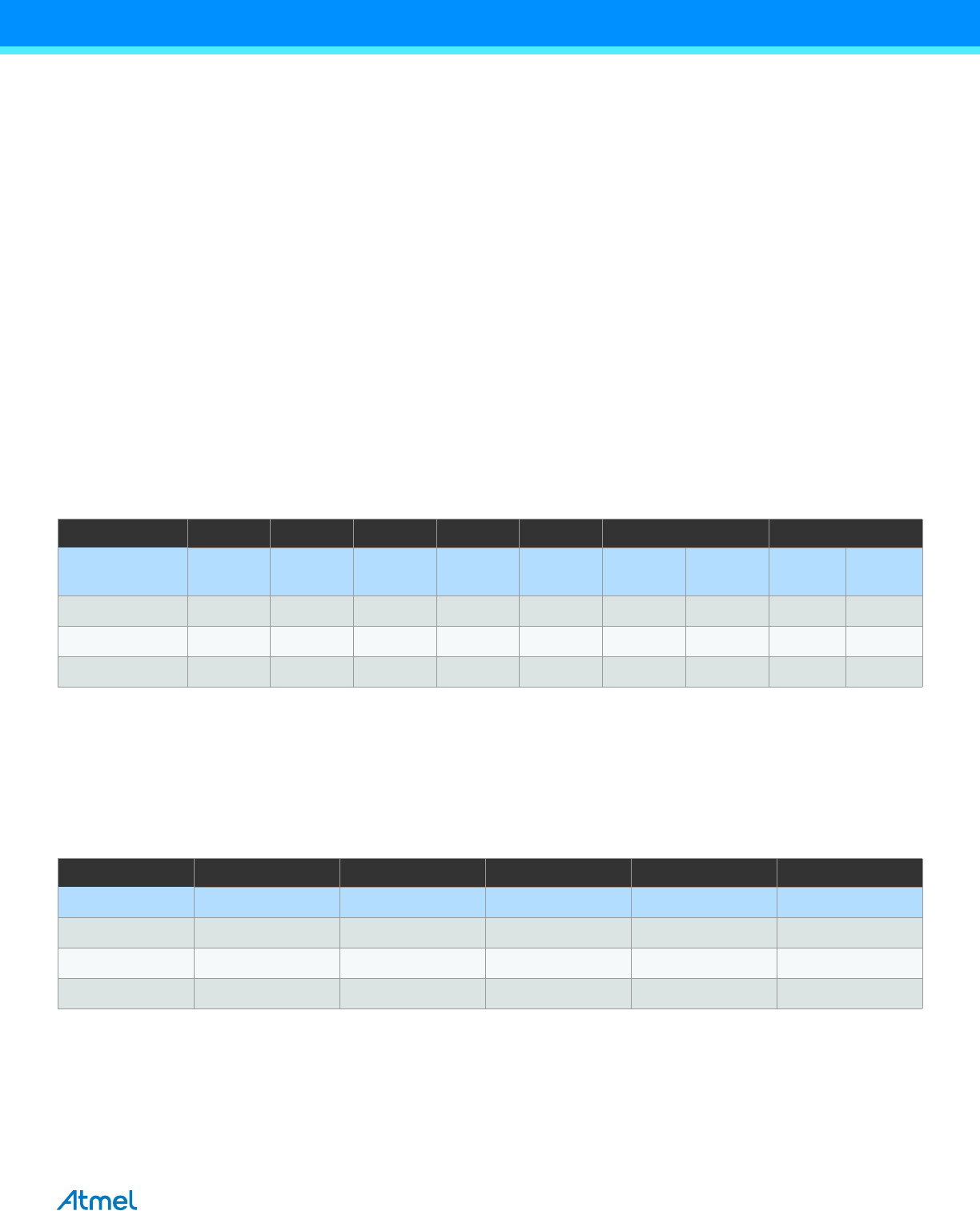
Table 8-2 shows the Flash Program Memory organization and Program Counter (PC) size. Flash write and erase
operations are performed on one page at a time, while reading the Flash is done one byte at a time. For Flash access the
Z-pointer (Z[m:n]) is used for addressing. The most significant bits in the address (FPAGE) give the page number and the
least significant address bits (FWORD) give the word in the page.
Table 8-2. Number of Words and Pages in the Flash
Table 8-3 shows EEPROM memory organization for the Atmel AVR XMEGA E5 devices. EEPROM write and erase
operations can be performed one page or one byte at a time, while reading the EEPROM is done one byte at a time. For
EEPROM access the NVM address register (ADDR[m:n]) is used for addressing. The most significant bits in the address
(E2PAGE) give the page number and the least significant address bits (E2BYTE) give the byte in the page.
Table 8-3. Number of Words and Pages in the EEPROM
Devices PC size Flash size Page Size FWORD FPAGE Application Boot
bits bytes words Size
No. of
pages
Size
No. of
pages
ATxmega32E5 15 32K+4K 64 Z[6:0] Z[14:7] 32K 256 4K 32
ATxmega16E5 14 16K+4K 64 Z[6:0] Z[13:7] 16K 128 4K 32
ATxmega8E5 13 8K+2K 64 Z[6:0] Z[12:7] 8K 64 2K 16
Devices EEPROM Page Size E2BYTE E2PAGE No. of Pages
Size bytes
ATxmega32E5 1K 32 ADDR[4:0] ADDR[10:5] 32
ATxmega16E5 512Bytes 32 ADDR[4:0] ADDR[10:5] 16
ATxmega8E5 512Bytes 32 ADDR[4:0] ADDR[10:5] 16