
Datasheet
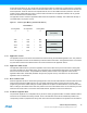
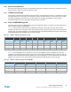

Table Of Contents
- Features
- 1. Ordering Information
- 2. Typical Applications
- 3. Pinout and Block Diagram
- 4. Overview
- 5. Resources
- 6. Capacitive Touch Sensing
- 7. CPU
- 8. Memories
- 9. EDMA – Enhanced DMA Controller
- 10. Event System
- 11. System Clock and Clock options
- 11.1 Features
- 11.2 Overview
- 11.3 Clock Sources
- 11.3.1 32kHz Ultra Low Power Internal Oscillator
- 11.3.2 32.768kHz Calibrated Internal Oscillator
- 11.3.3 32.768kHz Crystal Oscillator
- 11.3.4 0.4 - 16MHz Crystal Oscillator
- 11.3.5 8MHz Calibrated Internal Oscillator
- 11.3.6 32MHz Run-time Calibrated Internal Oscillator
- 11.3.7 External Clock Sources
- 11.3.8 PLL with 1x-31x Multiplication Factor
- 12. Power Management and Sleep Modes
- 13. System Control and Reset
- 14. WDT – Watchdog Timer
- 15. Interrupts and Programmable Multilevel Interrupt Controller
- 16. I/O Ports
- 17. Timer Counter Type 4 and 5
- 18. WeX – Waveform Extension
- 19. Hi-Res – High Resolution Extension
- 20. Fault Extension
- 21. RTC – 16-bit Real-Time Counter
- 22. TWI – Two-Wire Interface
- 23. SPI – Serial Peripheral Interface
- 24. USART
- 25. IRCOM – IR Communication Module
- 26. XCL – XMEGA Custom Logic Module
- 27. CRC – Cyclic Redundancy Check Generator
- 28. ADC – 12-bit Analog to Digital Converter
- 29. DAC – Digital to Analog Converter
- 30. AC – Analog Comparator
- 31. Programming and Debugging
- 32. Pinout and Pin Functions
- 33. Peripheral Module Address Map
- 34. Instruction Set Summary
- 35. Packaging Information
- 36. Electrical Characteristics
- 36.1 Absolute Maximum Ratings
- 36.2 General Operating Ratings
- 36.3 Current Consumption
- 36.4 Wake-up Time from Sleep Modes
- 36.5 I/O Pin Characteristics
- 36.6 ADC Characteristics
- 36.7 DAC Characteristics
- 36.8 Analog Comparator Characteristics
- 36.9 Bandgap and Internal 1.0V Reference Characteristics
- 36.10 External Reset Characteristics
- 36.11 Power-on Reset Characteristics
- 36.12 Flash and EEPROM Characteristics
- 36.13 Clock and Oscillator Characteristics
- 36.13.1 Calibrated 32.768kHz Internal Oscillator Characteristics
- 36.13.2 Calibrated 8MHz Internal Oscillator Characteristics
- 36.13.3 Calibrated and Tunable 32MHz Internal Oscillator Characteristics
- 36.13.4 32 kHz Internal ULP Oscillator Characteristics
- 36.13.5 Internal Phase Locked Loop (PLL) Characteristics
- 36.13.6 External Clock Characteristics
- 36.13.7 External 16MHz Crystal Oscillator and XOSC Characteristics
- 36.13.8 External 32.768kHz Crystal Oscillator and TOSC Characteristics
- 36.14 SPI Characteristics
- 36.15 Two-Wire Interface Characteristics
- 37. Typical Characteristics
- 37.1 Current Consumption
- 37.2 I/O Pin Characteristics
- 37.3 ADC Characteristics
- 37.4 DAC Characteristics
- 37.5 AC Characteristics
- 37.6 Internal 1.0V Reference Characteristics
- 37.7 BOD Characteristics
- 37.8 External Reset Characteristics
- 37.9 Power-on Reset Characteristics
- 37.10 Oscillator Characteristics
- 37.11 Two-wire Interface Characteristics
- 37.12 PDI Characteristics
- 38. Errata – ATxmega32E5 / ATxmega16E5 / ATxmega8E5
- 39. Revision History
- Table of Contents
14
XMEGA E5 [DATASHEET]
Atmel-8153J–AVR-ATxmega8E5-ATxmega16E5-ATxmega32E5_Datasheet–11/2014
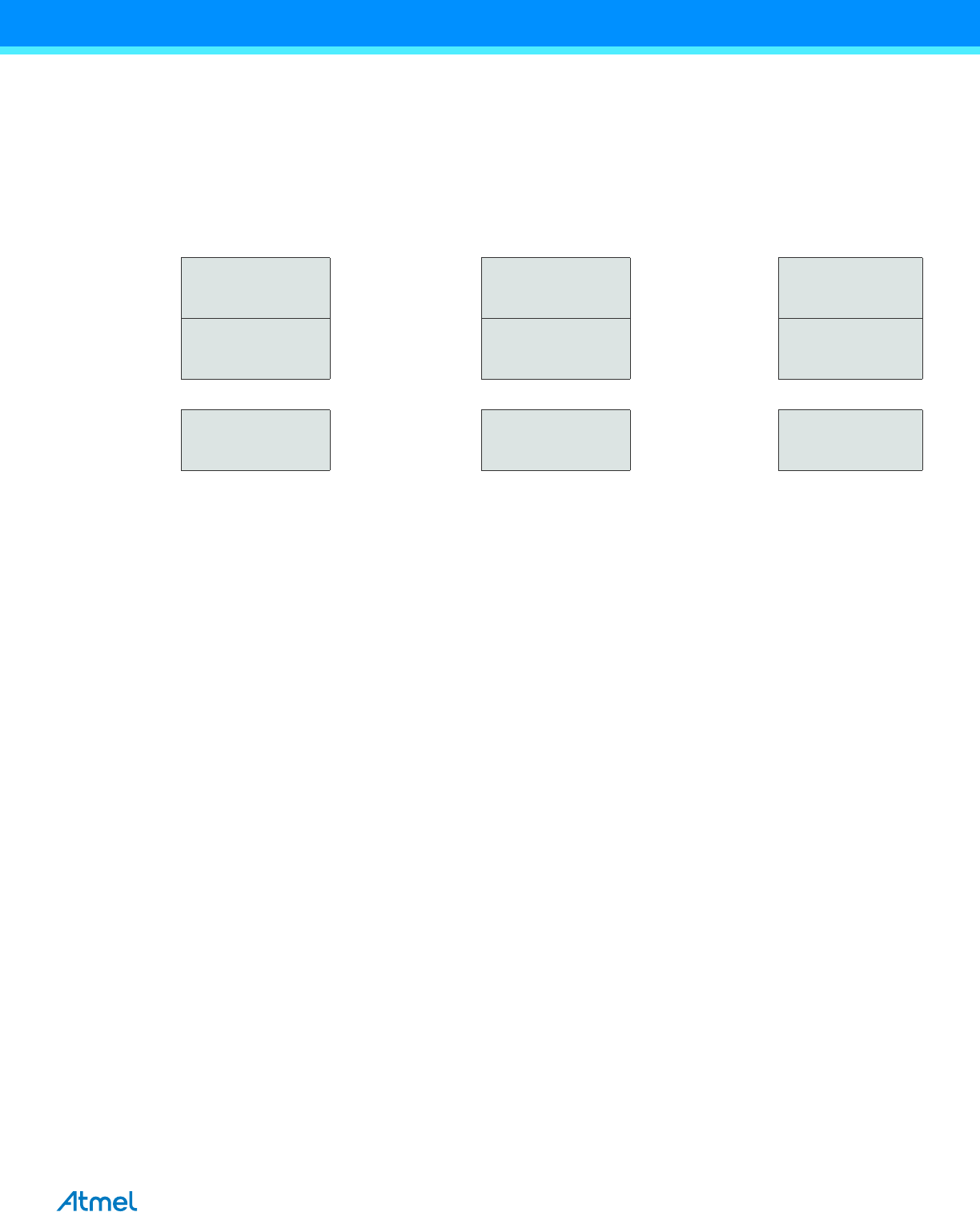
8.5 Data Memory
The data memory contains the I/O memory, internal SRAM and EEPROM. The data memory is organized as one
continuous memory section, see Table 8-2 on page 15. To simplify development, I/O Memory, EEPROM and SRAM will
always have the same start addresses for all XMEGA devices.
Figure 8-2. Data Memory Map (hexadecimal value)
8.6 EEPROM
Atmel AVR XMEGA E5 devices have EEPROM for nonvolatile data storage. It is memory mapped and accessed in
normal data space. The EEPROM supports both byte and page access. EEPROM allows highly efficient EEPROM
reading and EEPROM buffer loading. When doing this, EEPROM is accessible using load and store instructions.
EEPROM will always start at hexadecimal address 0x1000.
8.7 I/O Memory
The status and configuration registers for peripherals and modules, including the CPU, are addressable through I/O
memory locations. All I/O locations can be accessed by the load (LD/LDS/LDD) and store (ST/STS/STD) instructions,
which are used to transfer data between the 32 registers in the register file and the I/O memory. The IN and OUT
instructions can address I/O memory locations in the range of 0x00 to 0x3F directly. In the address range 0x00 - 0x1F,
single-cycle instructions for manipulation and checking of individual bits are available.
The I/O memory address for all peripherals and modules in XMEGA E5 is shown in the “Peripheral Module Address Map”
on page 61.
8.7.1 General Purpose I/O Registers
The lowest four I/O memory addresses are reserved as general purpose I/O registers. These registers can be used for
storing global variables and flags, as they are directly bit-accessible using the SBI, CBI, SBIS, and SBIC instructions.
8.8 Data Memory and Bus Arbitration
Since the data memory is organized as three separate sets of memories, the different bus masters (CPU, EDMA
controller read and EDMA controller write, etc.) can access different memory sections at the same time.
8.9 Memory Timing
Read and write access to the I/O memory takes one CPU clock cycle. A write to SRAM takes one cycle, and a read from
SRAM takes two cycles. For burst read (EDMA), new data are available every cycle. EEPROM page load (write) takes
one cycle, and three cycles are required for read. For burst read, new data are available every second cycle. Refer to the
instruction summary for more details on instructions and instruction timing.
Byte Address ATxmega32E5 Byte Address ATxmega16E5 Byte Address ATxmega8E5
0
I/O Registers (4K)
0
I/O Registers (4K)
0
I/O Registers (4K)
FFF FFF FFF
1000
EEPROM (1K)
1000
EEPROM (512B)
1000
EEPROM (512B)
13FF 11FF 11FF
RESERVED RESERVED RESERVED
2000
Internal SRAM (4K)
2000
Internal SRAM (2K)
2000
Internal SRAM (2K)
2FFF 27FF 27FF