
Datasheet
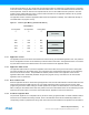
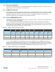

Table Of Contents
- Features
- 1. Ordering Information
- 2. Typical Applications
- 3. Pinout and Block Diagram
- 4. Overview
- 5. Resources
- 6. Capacitive Touch Sensing
- 7. CPU
- 8. Memories
- 9. EDMA – Enhanced DMA Controller
- 10. Event System
- 11. System Clock and Clock options
- 11.1 Features
- 11.2 Overview
- 11.3 Clock Sources
- 11.3.1 32kHz Ultra Low Power Internal Oscillator
- 11.3.2 32.768kHz Calibrated Internal Oscillator
- 11.3.3 32.768kHz Crystal Oscillator
- 11.3.4 0.4 - 16MHz Crystal Oscillator
- 11.3.5 8MHz Calibrated Internal Oscillator
- 11.3.6 32MHz Run-time Calibrated Internal Oscillator
- 11.3.7 External Clock Sources
- 11.3.8 PLL with 1x-31x Multiplication Factor
- 12. Power Management and Sleep Modes
- 13. System Control and Reset
- 14. WDT – Watchdog Timer
- 15. Interrupts and Programmable Multilevel Interrupt Controller
- 16. I/O Ports
- 17. Timer Counter Type 4 and 5
- 18. WeX – Waveform Extension
- 19. Hi-Res – High Resolution Extension
- 20. Fault Extension
- 21. RTC – 16-bit Real-Time Counter
- 22. TWI – Two-Wire Interface
- 23. SPI – Serial Peripheral Interface
- 24. USART
- 25. IRCOM – IR Communication Module
- 26. XCL – XMEGA Custom Logic Module
- 27. CRC – Cyclic Redundancy Check Generator
- 28. ADC – 12-bit Analog to Digital Converter
- 29. DAC – Digital to Analog Converter
- 30. AC – Analog Comparator
- 31. Programming and Debugging
- 32. Pinout and Pin Functions
- 33. Peripheral Module Address Map
- 34. Instruction Set Summary
- 35. Packaging Information
- 36. Electrical Characteristics
- 36.1 Absolute Maximum Ratings
- 36.2 General Operating Ratings
- 36.3 Current Consumption
- 36.4 Wake-up Time from Sleep Modes
- 36.5 I/O Pin Characteristics
- 36.6 ADC Characteristics
- 36.7 DAC Characteristics
- 36.8 Analog Comparator Characteristics
- 36.9 Bandgap and Internal 1.0V Reference Characteristics
- 36.10 External Reset Characteristics
- 36.11 Power-on Reset Characteristics
- 36.12 Flash and EEPROM Characteristics
- 36.13 Clock and Oscillator Characteristics
- 36.13.1 Calibrated 32.768kHz Internal Oscillator Characteristics
- 36.13.2 Calibrated 8MHz Internal Oscillator Characteristics
- 36.13.3 Calibrated and Tunable 32MHz Internal Oscillator Characteristics
- 36.13.4 32 kHz Internal ULP Oscillator Characteristics
- 36.13.5 Internal Phase Locked Loop (PLL) Characteristics
- 36.13.6 External Clock Characteristics
- 36.13.7 External 16MHz Crystal Oscillator and XOSC Characteristics
- 36.13.8 External 32.768kHz Crystal Oscillator and TOSC Characteristics
- 36.14 SPI Characteristics
- 36.15 Two-Wire Interface Characteristics
- 37. Typical Characteristics
- 37.1 Current Consumption
- 37.2 I/O Pin Characteristics
- 37.3 ADC Characteristics
- 37.4 DAC Characteristics
- 37.5 AC Characteristics
- 37.6 Internal 1.0V Reference Characteristics
- 37.7 BOD Characteristics
- 37.8 External Reset Characteristics
- 37.9 Power-on Reset Characteristics
- 37.10 Oscillator Characteristics
- 37.11 Two-wire Interface Characteristics
- 37.12 PDI Characteristics
- 38. Errata – ATxmega32E5 / ATxmega16E5 / ATxmega8E5
- 39. Revision History
- Table of Contents
13
XMEGA E5 [DATASHEET]
Atmel-8153J–AVR-ATxmega8E5-ATxmega16E5-ATxmega32E5_Datasheet–11/2014
the corresponding peripheral registers from software. For details on calibration conditions, refer to “Electrical
Characteristics” on page 71.
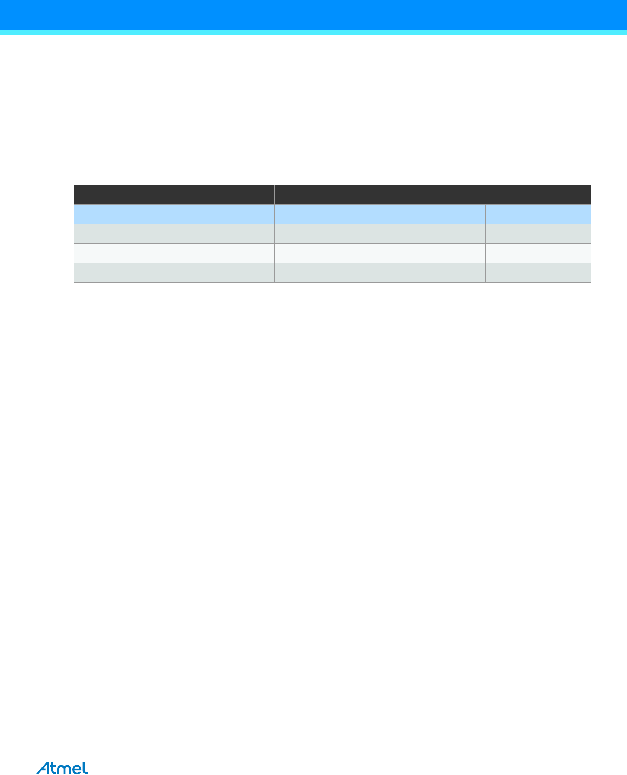
The production signature row also contains an ID that identifies each microcontroller device type and a serial number for
each manufactured device. The serial number consists of the production lot number, wafer number, and wafer
coordinates for the device. The device ID for the available devices is shown in Table 8-1.
The production signature row cannot be written or erased, but it can be read from application software and external
programmers.
Table 8-1. Device ID Bytes for Atmel AVR XMEGA E5 Devices
8.3.5 User Signature Row
The user signature row is a separate memory section that is fully accessible (read and write) from application software
and external programmers. It is one flash page in size, and is meant for static user parameter storage, such as calibration
data, custom serial number, identification numbers, random number seeds, etc. This section is not erased by chip erase
commands that erase the flash, and requires a dedicated erase command. This ensures parameter storage during
multiple program/erase operations and on-chip debug sessions.
8.4 Fuses and Lock Bits
The fuses are used to configure important system functions, and can only be written from an external programmer. The
application software can read the fuses. The fuses are used to configure reset sources such as brownout detector and
watchdog, startup configuration, etc.
The lock bits are used to set protection levels for the different flash sections (i.e., if read and/or write access should be
blocked). Lock bits can be written by external programmers and application software, but only to stricter protection levels.
Chip erase is the only way to erase the lock bits. To ensure that flash contents are protected even during chip erase, the
lock bits are erased after the rest of the flash memory has been erased.
An un-programmed fuse or lock bit will have the value one, while a programmed fuse or lock bit will have the value zero.
Both fuses and lock bits are reprogrammable like the flash program memory.
Device Device ID bytes
Byte 2 Byte 1 Byte 0
ATxmega32E5 4C 95 1E
ATxmega16E5 45 94 1E
ATxmega8E5 41 93 1E