
Datasheet
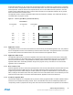

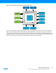
Table Of Contents
- Features
- 1. Ordering Information
- 2. Typical Applications
- 3. Pinout and Block Diagram
- 4. Overview
- 5. Resources
- 6. Capacitive Touch Sensing
- 7. CPU
- 8. Memories
- 9. EDMA – Enhanced DMA Controller
- 10. Event System
- 11. System Clock and Clock options
- 11.1 Features
- 11.2 Overview
- 11.3 Clock Sources
- 11.3.1 32kHz Ultra Low Power Internal Oscillator
- 11.3.2 32.768kHz Calibrated Internal Oscillator
- 11.3.3 32.768kHz Crystal Oscillator
- 11.3.4 0.4 - 16MHz Crystal Oscillator
- 11.3.5 8MHz Calibrated Internal Oscillator
- 11.3.6 32MHz Run-time Calibrated Internal Oscillator
- 11.3.7 External Clock Sources
- 11.3.8 PLL with 1x-31x Multiplication Factor
- 12. Power Management and Sleep Modes
- 13. System Control and Reset
- 14. WDT – Watchdog Timer
- 15. Interrupts and Programmable Multilevel Interrupt Controller
- 16. I/O Ports
- 17. Timer Counter Type 4 and 5
- 18. WeX – Waveform Extension
- 19. Hi-Res – High Resolution Extension
- 20. Fault Extension
- 21. RTC – 16-bit Real-Time Counter
- 22. TWI – Two-Wire Interface
- 23. SPI – Serial Peripheral Interface
- 24. USART
- 25. IRCOM – IR Communication Module
- 26. XCL – XMEGA Custom Logic Module
- 27. CRC – Cyclic Redundancy Check Generator
- 28. ADC – 12-bit Analog to Digital Converter
- 29. DAC – Digital to Analog Converter
- 30. AC – Analog Comparator
- 31. Programming and Debugging
- 32. Pinout and Pin Functions
- 33. Peripheral Module Address Map
- 34. Instruction Set Summary
- 35. Packaging Information
- 36. Electrical Characteristics
- 36.1 Absolute Maximum Ratings
- 36.2 General Operating Ratings
- 36.3 Current Consumption
- 36.4 Wake-up Time from Sleep Modes
- 36.5 I/O Pin Characteristics
- 36.6 ADC Characteristics
- 36.7 DAC Characteristics
- 36.8 Analog Comparator Characteristics
- 36.9 Bandgap and Internal 1.0V Reference Characteristics
- 36.10 External Reset Characteristics
- 36.11 Power-on Reset Characteristics
- 36.12 Flash and EEPROM Characteristics
- 36.13 Clock and Oscillator Characteristics
- 36.13.1 Calibrated 32.768kHz Internal Oscillator Characteristics
- 36.13.2 Calibrated 8MHz Internal Oscillator Characteristics
- 36.13.3 Calibrated and Tunable 32MHz Internal Oscillator Characteristics
- 36.13.4 32 kHz Internal ULP Oscillator Characteristics
- 36.13.5 Internal Phase Locked Loop (PLL) Characteristics
- 36.13.6 External Clock Characteristics
- 36.13.7 External 16MHz Crystal Oscillator and XOSC Characteristics
- 36.13.8 External 32.768kHz Crystal Oscillator and TOSC Characteristics
- 36.14 SPI Characteristics
- 36.15 Two-Wire Interface Characteristics
- 37. Typical Characteristics
- 37.1 Current Consumption
- 37.2 I/O Pin Characteristics
- 37.3 ADC Characteristics
- 37.4 DAC Characteristics
- 37.5 AC Characteristics
- 37.6 Internal 1.0V Reference Characteristics
- 37.7 BOD Characteristics
- 37.8 External Reset Characteristics
- 37.9 Power-on Reset Characteristics
- 37.10 Oscillator Characteristics
- 37.11 Two-wire Interface Characteristics
- 37.12 PDI Characteristics
- 38. Errata – ATxmega32E5 / ATxmega16E5 / ATxmega8E5
- 39. Revision History
- Table of Contents

12
XMEGA E5 [DATASHEET]
Atmel-8153J–AVR-ATxmega8E5-ATxmega16E5-ATxmega32E5_Datasheet–11/2014
All AVR CPU instructions are 16 or 32 bits wide, and each flash location is 16 bits wide. The flash memory is organized
in two main sections, the application section and the boot loader section. The sizes of the different sections are fixed, but
device-dependent. These two sections have separate lock bits, and can have different levels of protection. The store
program memory (SPM) instruction, which is used to write to the flash from the application software, will only operate
when executed from the boot loader section.
The application section contains an application table section with separate lock settings. This enables safe storage of
nonvolatile data in the program memory.
Figure 8-1. Flash Program Memory (hexadecimal address)
8.3.1 Application Section
The Application section is the section of the flash that is used for storing the executable application code. The protection
level for the application section can be selected by the boot lock bits for this section. The application section can not store
any boot loader code since the SPM instruction cannot be executed from the application section.
8.3.2 Application Table Section
The application table section is a part of the application section of the flash memory that can be used for storing data.
The size is identical to the boot loader section. The protection level for the application table section can be selected by
the boot lock bits for this section. The possibilities for different protection levels on the application section and the
application table section enable safe parameter storage in the program memory. If this section is not used for data,
application code can reside here.
8.3.3 Boot Loader Section
While the application section is used for storing the application code, the boot loader software must be located in the boot
loader section because the SPM instruction can only initiate programming when executing from this section. When
programming, the CPU is halted, waiting for the flash operation to complete. The SPM instruction can access the entire
flash, including the boot loader section itself. The protection level for the boot loader section can be selected by the boot
loader lock bits. If this section is not used for boot loader software, application code can be stored here.
8.3.4 Production Signature Row
The production signature row is a separate memory section for factory programmed data. It contains calibration data for
functions such as oscillators and analog modules. Some of the calibration values will be automatically loaded to the
corresponding module or peripheral unit during reset. Other values must be loaded from the signature row and written to
Word Address
ATxmega32E5 ATxmega16E5 ATxmega8E5
000
Application Section
(32K/16K/8K)
...
37FF / 17FF / BFF
3800 / 1800 / C00
Application Table Section
(4K/4K/2K)
3FFF / 1FFF / FFF
4000 / 2000 / 1000
Boot Section
(4K/4K/2K)
47FF / 27FF / 13FF