
Datasheet

75
XMEGA B1 [DATASHEET]
Atmel-8330H-AVR-ATxmega64B1-128B1_datasheet–12/2014
36.5 I/O Pin Characteristics
The I/O pins complies with the JEDEC LVTTL and LVCSMOS specification and the high- and low-level input and output
voltage limits reflect or exceed this specification.
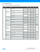
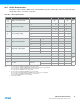
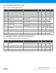
Table 36-7. I/O Pin Characteristics
Notes: 1. The sum of all I
OH
for PORTA and PORTB must not exceed 100mA.
The sum of all I
OH
for PORTC, PORTD, PORTE, and PDI must for each port not exceed 200mA.
The sum of all I
OH
for PORTG and PORTM must not exceed 100mA.
The sum of all I
OH
for PORTR must not exceed 100mA.
2. The sum of all I
OL
for PORTA and PORTB must not exceed 100mA.
The sum of all I
OL
for PORTC, PORTD, and PORTE must for each port not exceed 200mA.
The sum of all I
OL
for PORTG and PORTM must not exceed 100mA.
The sum of all I
OL
PORTR must not exceed 100mA.
3. From design simulations.
Symbol Parameter Condition Min. Typ. Max. Units
(1)
I
OH
/
(2)
I
OL
I/O pin source/sink current -20 20 mA
V
IH
High level input voltage
V
CC
= 3.0 - 3.6V 0.6*V
CC
V
CC
+0.3
V
V
CC
= 2.3 - 2.7V 0.6*V
CC
V
CC
+0.3
V
CC
= 1.6 - 2.3V 0.6*V
CC
V
CC
+0.3
V
IL
Low level input voltage
V
CC
= 3.0 - 3.6V -0.3 0.4*V
CC
V
CC
= 2.3 - 2.7V -0.3 0.4*V
CC
V
CC
= 1.6 - 2.3V -0.3 0.4*V
CC
V
OL
Output low voltage GPIO
V
CC
= 3.3V I
OL
= 15mA 0.4 0.76
V
CC
= 3.0V I
OL
= 10mA 0.26 0.64
V
CC
= 1.8V I
OL
= 5mA 0.17 0.46
V
OH
Output high voltage GPIO
V
CC
= 3.3V I
OH
= -8mA 2.6 2.8
V
CC
= 3.0V I
OH
= -6mA 2.1 2.6
V
CC
= 1.8V I
OH
= -2mA 1.4 1.6
I
IN
Input leakage current I/O pin <0.01 1 µA
R
P
Pull/Buss keeper resistor 25
k
R
RST
Reset pin pull-up resistor 25
(3)
t
r
Rise time No load
4
ns
slew rate limitation 7