Atmel AVR XMEGA B1 8- and 16-bit Microcontroller ATxmega128B1 / ATxmega64B1 Features High-performance, low-power Atmel® AVR® XMEGA® 8- and16-bit Microcontroller Nonvolatile program and data memories 64K - 128KBytes of in-system self-programmable flash 4K - 8KBytes boot section 2KBytes EEPROM 4K - 8KBytes internal SRAM Peripheral features Two-channel DMA controller Four-channel event system Three 16-bit timer/counters Two timer/counters with four output compare or input capture chann
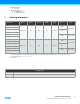
Operating voltage 1.6 – 3.6V Operating frequency 0 – 12MHz from 1.6V 0 – 32MHz from 2.7V 1. Ordering Information Flash [Bytes] Ordering Code EEPROM [Bytes] SRAM [Bytes] Speed [MHz] Power supply Package(1)(2)(3) Temp. ATxmega128B1-AU 100A ATxmega128B1-AUR(4) -40C - 85C ATxmega128B1-CU 128K + 8K 2K 8K 32 1.6 - 3.
Typical Applications Industrial control Climate control Low power battery applications Factory automation RF and ZigBee® Power tools Building control USB connectivity HVAC Board control Sensor control Utility metering White goods Optical Medical applications XMEGA B1 [DATASHEET] Atmel-8330H-AVR-ATxmega64B1-128B1_datasheet–12/2014 3
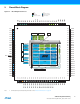
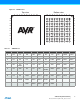
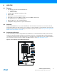
2. Pinout/Block Diagram Figure 2-1.
Figure 2-2. VFBGA Pinout Top view 1 2 3 4 5 6 Bottom view 7 8 9 10 10 9 8 7 6 5 4 3 2 1 A A B B C C D D E E F F G G H H J J K K Table 2-1.
3. Overview The Atmel® AVR® XMEGA® is a family of low power, high performance, and peripheral rich 8/16-bit microcontrollers based on the AVR enhanced RISC architecture. By executing instructions in a single clock cycle, the Atmel AVR XMEGA devices achieve CPU throughput approaching one million instructions per second (MIPS) per megahertz, allowing the system designer to optimize power consumption versus processing speed.
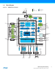
3.1 Block Diagram Figure 3-1. XMEGA B1 Block Diagram PR[0..1] XTAL1 / TOSC1 Power LCD Ground Programming, debug, test Digital function External clock / Crystal pins Analog function / Oscillators General Purpose I/O XTAL2 / TOSC2 Oscillator Circuits/ Clock Generation PORT R (2) Real Time Counter Watchdog Oscillator EVENT ROUTING NETWORK DATA BUS PA[0..
4. Resources A comprehensive set of development tools, application notes and datasheets are available for download on http://www.atmel.com/avr. 4.1 Recommended Reading XMEGA B Manual XMEGA Application Notes This device data sheet only contains part specific information with a short description of each peripheral and module. The XMEGA B Manual describes the modules and peripherals in depth. The XMEGA application notes contain example code and show applied use of the modules and peripherals.
6. AVR CPU 6.1 Features 8/16-bit, high-performance Atmel AVR RISC CPU 142 instructions Hardware multiplier 32x8-bit registers directly connected to the ALU Stack in RAM Stack pointer accessible in I/O memory space Direct addressing of up to 16MB of program memory and 16MB of data memory True 16/24-bit access to 16/24-bit I/O registers Efficient support for 8-, 16-, and 32-bit arithmetic Configuration change protection of system-critical features 6.
The Arithmetic Logic Unit (ALU) supports arithmetic and logic operations between registers or between a constant and a register. Single-register operations can also be executed in the ALU. After an arithmetic operation, the status register is updated to reflect information about the result of the operation. The ALU is directly connected to the fast-access register file.
6.5 Program Flow After reset, the CPU starts to execute instructions from the lowest address in the flash program memory ‘0.’ The program counter (PC) addresses the next instruction to be fetched. Program flow is provided by conditional and unconditional jump and call instructions capable of addressing the whole address space directly. Most AVR instructions use a 16-bit word format, while a limited number use a 32-bit format.
7. Memories 7.
7.3 Flash Program Memory The Atmel AVR XMEGA devices contain on-chip, in-system re-programmable flash memory for program storage. The flash memory can be accessed for read and write from an external programmer through the PDI or from application software running in the device. All AVR CPU instructions are 16- or 32-bits wide, and each flash location is 16 bits wide. The flash memory is organized in two main sections, the application section and the boot loader section.
7.3.4 Production Signature Row The production signature row is a separate memory section for factory programmed data. It contains calibration data for functions such as oscillators and analog modules. Some of the calibration values will be automatically loaded to the corresponding module or peripheral unit during reset. Other values must be loaded from the signature row and written to the corresponding peripheral registers from software.
Figure 7-2. Data Memory Map (hexadecimal address) Byte Address ATxmega128B1 0 Byte Address ATxmega64B1 0 I/O Registers (4K) FFF I/O Registers (4KB) FFF 1000 1000 EEPROM (2K) 17FF EEPROM (2K) 17FF RESERVED 2000 RESERVED 2000 Internal SRAM (8K) 3FFF 7.6 Internal SRAM (4K) 2FFF EEPROM Atmel AVR XMEGA B1 devices have EEPROM for nonvolatile data storage. It is either addressable in a separate data space (default) or memory mapped and accessed in normal data space.
7.11 JTAG Disable It is possible to disable the JTAG interface from the application software. This will prevent all external JTAG access to the device until the next device reset or until JTAG is enabled again from the application software. As long as JTAG is disabled, the I/O pins required for JTAG can be used as normal I/O pins. 7.12 I/O Memory Protection Some features in the device are regarded as critical for safety in some applications.
8. DMAC – Direct Memory Access Controller 8.
9. Event System 9.
Figure 9-1. Event System Overview and Connected Peripherals CPU / Software DMA Controller Event Routing Network ADC AC clkPER Prescaler Real Time Counter Event System Controller Timer / Counters USB Port pins IRCOM The event routing network consists of four software-configurable multiplexers that control how events are routed and used. These are called event channels, and allow for up to four parallel event configurations and routings. The maximum routing latency is two peripheral clock cycles.
10. System Clock and Clock Options 10.1 Features Fast start-up time Safe run-time clock switching Internal oscillators: 32MHz run-time calibrated oscillator 2MHz run-time calibrated oscillator 32.768kHz calibrated oscillator 32kHz Ultra Low Power (ULP) oscillator with 1kHz output External clock options 0.4MHz - 16MHz crystal oscillator 32.
Figure 10-1. The Clock System, Clock Sources, and Clock Distribution Real Time Counter LCD Peripherals RAM Non-Volatile Memory AVR CPU clkPER clkCPU clkPER2 clkPER4 clkRTC clkLCD USB clkUSB System Clock Prescalers Watchdog Timer Prescaler clkSYS Brown-out Detector System Clock Multiplexer (SCLKSEL) DIV32 DIV32 DIV32 RTCSRC USBSRC PLL DIV4 PLLSRC 10.3 XTAL2 0.4 – 16 MHz XTAL XTAL1 32.768 kHz TOSC TOSC2 32.768 kHz Int. OSC TOSC1 32 kHz Int. ULP 32 MHz Int. Osc 2 MHz Int.
10.3.2 32.768kHz Calibrated Internal Oscillator This oscillator provides an approximate 32.768kHz clock. It is calibrated during production to provide a default frequency close to its nominal frequency. The calibration register can also be written from software for run-time calibration of the oscillator frequency. The oscillator employs a built-in prescaler, which provides both a 32.768kHz output and a 1.024kHz output.
11. Power Management and Sleep Modes 11.1 Features Power management for adjusting power consumption and functions Five sleep modes Idle Power down Power save Standby Extended standby Power reduction register to disable clock and turn off unused peripherals in active and idle modes 11.2 Overview Various sleep modes and clock gating are provided in order to tailor power consumption to application requirements.
11.3.3 Power-save Mode Power-save mode is identical to power down, with two exceptions: 1. If the real-time counter (RTC) is enabled, it will keep running during sleep, and the device can also wake up from either an RTC overflow or compare match interrupt. 2. If the liquid crystal display controller (LCD) is enabled, it will keep running during sleep, and the device can wake up from LCD frame completed interrupt. 11.3.
12. System Control and Reset 12.1 Features Reset the microcontroller and set it to initial state when a reset source goes active Multiple reset sources that cover different situations Power-on reset External reset Watchdog reset Brownout reset PDI reset Software reset Asynchronous operation No running system clock in the device is required for reset Reset status register for reading the reset source from the application code 12.
12.4.2 Brownout Detection The on-chip brownout detection (BOD) circuit monitors the VCC level during operation by comparing it to a fixed, programmable level that is selected by the BODLEVEL fuses. If disabled, BOD is forced on at the lowest level during chip erase and when the PDI is enabled. 12.4.3 External Reset The external reset circuit is connected to the external RESET pin.
13. WDT – Watchdog Timer 13.1 Features Issues a device reset if the timer is not reset before its timeout period Asynchronous operation from dedicated oscillator 1kHz output of the 32kHz ultra low power oscillator 11 selectable timeout periods, from 8ms to 8s Two operation modes: Normal mode Window mode Configuration lock to prevent unwanted changes 13.2 Overview The watchdog timer (WDT) is a system function for monitoring correct program operation.
14. Interrupts and Programmable Multilevel Interrupt Controller 14.
Program address (Base address) Source Interrupt description 0x028 TCC1_INT_base Timer/Counter 1 on port C Interrupt base 0x030 SPIC_INT_vect SPI on port C Interrupt vector 0x032 USARTC0_INT_base USART 0 on port C Interrupt base 0x03E USB_INT_base USB on port D Interrupt base 0x046 LCD_INT_base LCD Interrupt base 0x048 AES_INT_vect AES Interrupt vector 0x04A NVM_INT_base Non-Volatile Memory Interrupt base 0x04E PORTB_INT_base Port B Interrupt base 0x052 ACB_INT_base Analog Compar
15. I/O Ports 15.
15.3.1 Push-pull Figure 15-1. I/O Configuration - Totem-pole DIRn OUTn Pn INn 15.3.2 Pull-down Figure 15-2. I/O Configuration - Totem-pole with Pull-down (on Input) DIRn OUTn Pn INn 15.3.3 Pull-up Figure 15-3. I/O Configuration - Totem-pole with Pull-up (on Input) DIRn OUTn Pn INn 15.3.4 Bus-keeper The bus-keeper’s weak output produces the same logical level as the last output level. It acts as a pull-up if the last level was ‘1’, and pull-down if the last level was ‘0’.
Figure 15-4. I/O Configuration - Totem-pole with Bus-keeper DIRn OUTn Pn INn 15.3.5 Others Figure 15-5. Output Configuration - Wired-OR with Optional Pull-down OUTn Pn INn Figure 15-6.
15.4 Input Sensing Input sensing is synchronous or asynchronous depending on the enabled clock for the ports, and the configuration is shown in Figure 15-7 on page 33. Figure 15-7. Input Sensing System Overview Asynchronous sensing EDGE DETECT Interrupt Control IREQ Synchronous sensing Pn Synchronizer INn D Q D Q INVERTED I/O R EDGE DETECT Event R When a pin is configured with inverted I/O, the pin value is inverted before the input sensing. 15.
16. T/C – 16-bit Timer/Counter Type 0 and 1 16.
Only Timer/Counter 0 has the split mode feature that split it into two 8-bit Timer/Counters with four compare channels each. Some timer/counters have extensions to enable more specialized waveform and frequency generation. The advanced waveform extension (AWeX) is intended for motor control and other power control applications. It enables low- and highside output with dead-time insertion, as well as fault protection for disabling and shutting down external drivers.
17. TC2 –16-bit Timer/Counter Type 2 17.
18. AWeX – Advanced Waveform Extension 18.
19. Hi-Res – High Resolution Extension 19.1 Features Increases waveform generator resolution up to 8x (three bits) Supports frequency, single-slope PWM, and dual-slope PWM generation Supports the AWeX when this is used for the same timer/counter 19.2 Overview The high-resolution (hi-res) extension can be used to increase the resolution of the waveform generation output from a timer/counter by four or eight.
20. RTC – 16-bit Real-Time Counter 20.1 Features 16-bit resolution Selectable clock source 32.768kHz external crystal External clock 32.768kHz internal oscillator 32kHz internal ULP oscillator Programmable 10-bit clock prescaling One compare register One period register Clear counter on period overflow Optional interrupt/event on overflow and compare match 20.
21. USB – Universal Serial Bus Interface 21.1 Features One USB 2.0 full speed (12Mbps) and low speed (1.
Multi-packet transfer enables a data payload exceeding the maximum packet size of an endpoint to be transferred as multiple packets without software intervention. This reduces the CPU intervention and the interrupts needed for USB transfers. For low-power operation, the USB module can put the microcontroller into any sleep mode when the USB bus is idle and a suspend condition is given. Upon bus resumes, the USB module can wake up the microcontroller from any sleep mode. PORTD has one USB.
22. TWI – Two-wire Interface 22.
23. SPI – Serial Peripheral Interface 23.1 Features One SPI peripheral Full-duplex, three-wire synchronous data transfer Master or slave operation LSB first or MSB first data transfer Eight programmable bit rates Interrupt flag at the end of transmission Write collision flag to indicate data collision Wake up from idle sleep mode Double speed master mode 23.2 Overview The Serial Peripheral Interface (SPI) is a high-speed synchronous data transfer interface using three or four pins.
24. USART 24.
25. IRCOM – IR Communication Module 25.1 Features Pulse modulation/demodulation for infrared communication IrDA compatible for baud rates up to 115.2kbps Selectable pulse modulation scheme 3/16 of the baud rate period Fixed pulse period, 8-bit programmable Pulse modulation disabled Built-in filtering Can be connected to and used by any USART 25.2 Overview XMEGA devices contain an infrared communication module (IRCOM) that is IrDA compatible for baud rates up to 115.2kbps.
26. AES and DES Crypto Engine 26.1 Features Data Encryption Standard (DES) CPU instruction Advanced Encryption Standard (AES) crypto module DES Instruction Encryption and decryption DES supported Encryption/decryption in 16 CPU clock cycles per 8-byte block AES crypto module Encryption and decryption Supports 128-bit keys Supports XOR data load mode to the state memory Encryption/decryption in 375 clock cycles per 16-byte block 26.
27. CRC – Cyclic Redundancy Check Generator 27.
28. LCD - Liquid Crystal Display Controller 28.
29. ADC – 12-bit Analog to Digital Converter 29.1 Features Two Analog to Digital Converters (ADCs) 12-bit resolution Up to three hundred thousand samples per second Down to 2.3µs conversion time with 8-bit resolution Down to 3.
Figure 29-1. ADC Overview ADC0 • • • ADC15 Compare Register ADC Internal signals ADC0 • • • ADC7 < > VINP Threshold (Int Req) CH0 Result VINN Internal 1.00V Internal AVCC/1.6V Internal AVCC/2 AREFA AREFB Reference Voltage The ADC may be configured for 8- or 12-bit result, reducing the minimum conversion time (propagation delay) from 3.35µs for 12-bit to 2.3µs for 8-bit result. ADC conversion results are provided left- or right adjusted with optional ‘1’ or ‘0’ padding.
30. AC – Analog Comparator 30.
Figure 30-1. Analog Comparator Overview Pin Input + AC0 - Pin Input AC0OUT Hysteresis Enable Voltage Scaler ACnMUXCTRL ACnCTRL Interrupt Mode WINCTRL Enable Bandgap Interrupt Sensititivity Control & Window Function Interrupts Events Hysteresis + AC1 - Pin Input AC1OUT Pin Input The window function is realized by connecting the external inputs of the two analog comparators in a pair as shown in Figure 30-2. Figure 30-2.
31. Programming and Debugging 31.
32. Pinout and Pin Functions The device pinout is shown in “Pinout/Block Diagram” on page 4. In addition to general purpose I/O functionality, each pin can have several alternate functions. This will depend on which peripheral is enabled and connected to the actual pin. Only one of the pin functions can be used at time. 32.1 Alternate Pin Function Description The tables below show the notation for all pin functions available and describe its function. 32.1.
32.1.5 Timer/Counter and AWEX Functions OCnxLS Output Compare Channel x Low Side for Timer/Counter n OCnxHS Output Compare Channel x High Side for Timer/Counter n 32.1.
32.2 TCK JTAG Test Clock TDI JTAG Test Data In TDO JTAG Test Data Out TMS JTAG Test Mode Select Alternate Pin Functions The tables below show the primary/default function for each pin on a port in the first column, the pin number in the second column, and then all alternate pin functions in the remaining columns. The head row shows what peripheral that enable and use the alternate pin functions.
Table 32-3.
Table 32-6. Port E - Alternate Functions PIN # INTERRUPT TCE0(1) PE0 19 SYNC OC0A PE1 20 SYNC OC0B XCK0 PE2 21 SYNC/ASYNC OC0C RXD0 PE3 22 SYNC OC0D TXD0 PE4 23 SYNC PE5 24 SYNC PE6 25 SYNC PE7 26 SYNC PORT E USARTE0(2) CLOCKOUT(4) EVENTOUT(5) Alternate TOSC TOSC2 clkPER EVOUT TOSC1 Table 32-7.
LCD(1)(2) PIN # INTERRUPT(1) GPIO(1) BLINK(1) SEG18 50 SEG17 51 SEG16 52 SEG15 53 SEG14 54 SEG13 55 SEG12 56 SEG11 57 SEG10 58 SEG9 59 SEG8 60 SEG7 61 SEG6 62 SEG5 63 SEG4 64 SEG3 65 SEG2 66 SEG1 67 BLINK SEG0 68 BLINK GND 69 VCC 70 BIAS1 71 BIAS2 72 VLCD 73 CAPL 74 CAPH 75 COM0 76 COM1 77 COM2 78 COM3 79 Notes: 1. 2. Pin mapping of all Segment terminals (SEGn) can be optionally swapped.
33. Peripheral Module Address Map The address maps show the base address for each peripheral and module in XMEGA B1. For complete register description and summary for each peripheral module, refer to the XMEGA B Manual. Table 33-1.
Base address Name Description 0x0800 TCC0 Timer/Counter 0 on port C 0x0840 TCC1 Timer/Counter 1 on port C 0x0880 AWEXC Advanced Waveform Extension on port C 0x0890 HIRESC High Resolution Extension on port C 0x08A0 USARTC0 0x08C0 SPIC 0x08F8 IRCOM 0x0A00 TCE0 0x0AA0 USARTE0 0x0D00 LCD USART 0 on port C Serial Peripheral Interface on port C Infrared Communication Module Timer/Counter 0 on port E USART 0 on port E Liquid Crystal Display XMEGA B1 [DATASHEET] Atmel-8330H-AVR-ATxmega64
34.
Mnemonics Operands Description RCALL k Relative Call Subroutine Operation Flags #Clocks PC PC + k + 1 None 2 / 3 (1) ICALL Indirect Call to (Z) PC(15:0) PC(21:16) Z, 0 None 2 / 3 (1) EICALL Extended Indirect Call to (Z) PC(15:0) PC(21:16) Z, EIND None 3 (1) call Subroutine PC k None 3 / 4 (1) RET Subroutine Return PC STACK None 4 / 5 (1) RETI Interrupt Return PC STACK I 4 / 5 (1) if (Rd = Rr) PC PC + 2 or 3 None 1/2/3 CALL k CPSE Rd,R
Mnemonics Operands Description MOVW Rd, Rr Copy Register Pair LDI Rd, K Load Immediate Operation Flags #Clocks 1 Rd+1:Rd Rr+1:Rr None Rd K None 1 (1)(2) LDS Rd, k Load Direct from data space Rd (k) None 2 LD Rd, X Load Indirect Rd (X) None 1 (1)(2) LD Rd, X+ Load Indirect and Post-Increment Rd X (X) X+1 None 1 (1)(2) LD Rd, -X Load Indirect and Pre-Decrement X X - 1, Rd (X) X-1 (X) None 2 (1)(2) LD Rd, Y Load Indirect Rd (Y) (
Mnemonics Operands Description ELPM Rd, Z Extended Load Program Memory Rd ELPM Rd, Z+ Extended Load Program Memory and PostIncrement Rd Z Store Program Memory SPM Operation Flags #Clocks (RAMPZ:Z) None 3 (RAMPZ:Z), Z+1 None 3 (RAMPZ:Z) R1:R0 None - (RAMPZ:Z) Z R1:R0, Z+2 None - Rd I/O(A) None 1 I/O(A) Rr None 1 STACK Rr None 1 (1) SPM Z+ Store Program Memory and Post-Increment by 2 IN Rd, A In From I/O Location OUT A, Rr Out To I/O L
Mnemonics Operands Description Operation Flags #Clocks SEN Set Negative Flag N 1 N 1 CLN Clear Negative Flag N 0 N 1 SEZ Set Zero Flag Z 1 Z 1 CLZ Clear Zero Flag Z 0 Z 1 SEI Global Interrupt Enable I 1 I 1 CLI Global Interrupt Disable I 0 I 1 SES Set Signed Test Flag S 1 S 1 CLS Clear Signed Test Flag S 0 S 1 SEV Set Two’s Complement Overflow V 1 V 1 CLV Clear Two’s Complement Overflow V 0 V 1 SET Set T in SREG
35. Packaging Information 35.1 100A PIN 1 B PIN 1 IDENTIFIER E1 e E D1 D C 0°~7° A1 A2 A L COMMON DIMENSIONS (Unit of Measure = mm) MIN NOM MAX A – – 1.20 A1 0.05 – 0.15 A2 0.95 1.00 1.05 D 15.75 16.00 16.25 D1 13.90 14.00 14.10 SYMBOL Notes: 1. This package conforms to JEDEC reference MS-026, Variation AED. 2. Dimensions D1 and E1 do not include mold protrusion. Allowable protrusion is 0.25mm per side.
35.
36. Electrical Characteristics All typical values are measured at T = 25°C unless other temperature condition is given. All minimum and maximum values are valid across operating temperature and voltage unless other conditions are given. 36.1 Absolute Maximum Ratings Stresses beyond those listed in Table 36-1 on page 69 under may cause permanent damage to the device.
Figure 36-1. Maximum Frequency vs. VCC MHz 32 Safe Operating Area 12 1.6 1.8 2.7 3.
36.3 DC Characteristics Table 36-4. Current Consumption for Active and Sleep Modes Symbol Parameter Condition 32kHz, Ext. Clk Active Power consumption(1) 1MHz, Ext. Clk 2MHz, Ext. Clk 32MHz, Ext. Clk 32kHz, Ext. Clk Idle Power consumption(1) 1MHz, Ext. Clk 2MHz, Ext. Clk ICC 32MHz, Ext. Clk Min. T = 85°C WDT and Sampled BOD enabled, T = 25°C 150 VCC = 3.0V 320 VCC = 1.8V 350 VCC = 3.0V 700 VCC = 1.8V 650 800 1.0 1.6 10 15 VCC = 3.0V Power-save power consumption(2) mA 4.
Symbol Parameter Power-save power consumption(2) ICC Reset power consumption Notes: 1. 2. Condition Min. Typ. RTC on ULP clock, WDT, sampled BOD and LCD enabled, and all pixels ON, T = 25°C VCC = 1.8V 4.6 VCC = 3.0V 5.2 RTC on 1.024kHz low power 32.768kHz TOSC, LCD enabled and all pixels ON T = 25°C VCC = 1.8V 3.9 VCC = 3.0V 4.3 RTC from low power 32.768kHz TOSC, LCD enabled and all pixels ON, T = 25°C VCC = 1.8V 4.0 VCC = 3.0V 4.5 Current through RESET pin substracted VCC = 3.
Table 36-5. Current Consumption for Modules and Peripherals Symbol Parameter Condition(1) Min. Typ. ULP oscillator 1.0 32.768kHz int. oscillator 26 2MHz int. oscillator Max. Units 80 DFLL enabled with 32.768kHz int. osc. as reference 112 255 32MHz int. oscillator DFLL enabled with 32.768kHz int. osc. as reference 444 PLL Multiplication factor = 20x 316 Watchdog Timer 1 Continuous mode 126 Sampled mode, include ULP oscillator 1.
Symbol Parameter Condition(1) Min. AC ICC 1. 2. 36.4 Max. Units 440 DMA 615Kbps between I/O registers and SRAM USART Rx and Tx enabled, 9600 BAUD 115 µA 9 Flash memory and EEPROM programming Notes: Typ. 4.4 mA All parameters measured as the difference in current consumption between module enabled and disabled. All data at VCC = 3.0V, ClkSYS = 1MHz External clock without prescaling, T = 25°C unless other conditions are given.
36.5 I/O Pin Characteristics The I/O pins complies with the JEDEC LVTTL and LVCSMOS specification and the high- and low-level input and output voltage limits reflect or exceed this specification. Table 36-7. I/O Pin Characteristics Symbol (1) IOH/ IOL Parameter Condition Min. Max. Units -20 20 mA VCC = 3.0 - 3.6V 0.6*VCC VCC+0.3 VCC = 2.3 - 2.7V 0.6*VCC VCC+0.3 VCC = 1.6 - 2.3V 0.6*VCC VCC+0.3 VCC = 3.0 - 3.6V -0.3 0.4*VCC VCC = 2.3 - 2.7V -0.3 0.4*VCC VCC = 1.6 - 2.3V -0.3 0.
36.6 Liquid Crystal Display Characteristics Table 36-8. Symbol Liquid Crystal Display Characteristics Parameter Condition Min. Typ. Max. SEG Segment terminal pins 0 40 COM Common terminal pins 0 4 fFrame LCD frame frequency 31.25 512 CFlying Flying capacitor Contrast 100 Contrast adjustment VLCD BIAS2 F(clkLCD)=32.768kHz LCD regulated voltages BIAS1 -0.5 COM0 to COM3 RSEG Segment output impedance SEG0 to SEG39(1) Notes: 1. 36.7 ADC Characteristics nF 0.
Symbol Parameter Condition Min. Current limitation (CURRLIMIT) off fADC Typ. 16 Max. Units 300 CURRLIMIT = LOW 250 CURRLIMIT = MEDIUM 150 CURRLIMIT = HIGH 50 Sample rate ksps Sampling time 1/2 ClkADC cycle 0.25 5 Conversion time (latency) (RES+2)/2+(GAIN !=0) RES (Resolution) = 8 or 12 6 10 Start-up time ADC clock cycles 12 24 ADC settling time After changing reference or input mode 7 7 Min. Typ. Max.
Symbol Condition(2) Parameter Gain error Min. 1. 2. Units -5 AVCC/1.6 -5 AVCC/2.0 -6 Bandgap ±10 Temperature drift 0.02 mV/K 2 mV/V Differential mode mV External reference -8 AVCC/1.6 -8 AVCC/2.0 -8 Bandgap ±10 Temperature drift 0.03 mV/K 2 mV/V Single ended unsigned mode mV Operating voltage drift Notes: Max. External reference Operating voltage drift Gain error Typ.
36.8 Analog Comparator Characteristics Table 36-13. Analog Comparator Characteristics Symbol Voff Ilk Parameter Condition Min. Typ. Input offset voltage 10 Input leakage current <10 Input voltage range 0.1 AC startup time Max. Units mV 50 nA AVCC- 0.1 V 50 µs Vhys1 Hysteresis, none VCC = 1.6V - 3.6V 0 Vhys2 Hysteresis, small VCC = 1.6V - 3.6V 12 Vhys3 Hysteresis, large VCC = 1.6V - 3.6V 28 30 Propagation delay VCC = 3.0V, T= 85°C 22 tdelay VCC = 1.6V - 3.6V 21 40 0.
36.10 Brownout Detection Characteristics Table 36-15. Brownout Detection Characteristics(1) Symbol Parameter Condition BOD level 0 falling VCC T = 85C, calibrated Min. Typ. Max. 1.5 1.6 1.72 BOD level 1 falling VCC 1.8 BOD level 2 falling VCC 2.0 BOD level 3 falling VCC 2.2 BOD level 4 falling VCC 2.4 BOD level 5 falling VCC 2.6 BOD level 6 falling VCC 2.8 BOD level 7 falling VCC 3.0 V Continuous mode tBOD Note: 0.4 Detection time µs Sampled mode VHYST 1000 Hysteresis 1.
36.13 Flash and EEPROM Memory Characteristics Table 36-18. Endurance and Data Retention Symbol Parameter Condition Min. 25°C 10K 85°C 10K 25°C 100 55°C 25 25°C 100K 85°C 100K 25°C 100 55°C 25 Typ. Max. Write/erase cycles Units Cycle Flash Data retention Year Write/erase cycles Cycle EEPROM Data retention Year Table 36-19. Programming Time Symbol Parameter Chip Erase Flash EEPROM Notes: 1. 2. Condition Min. Typ.
36.14.2 Calibrated 2MHz RC Internal Oscillator Characteristics Table 36-21. Calibrated 2MHz Internal Oscillator Characteristics Symbol Parameter Frequency range Condition Min. DFLL can tune to this frequency over voltage and temperature 1.8 Factory calibrated frequency Factory calibration accuracy Typ. Max. Units 2.2 MHz 2.0 T = 85C, VCC= 3.0V User calibration accuracy MHz -1.5 1.5 % -0.2 0.2 % DFLL calibration step size 0.22 % 36.14.
36.14.6 External Clock Characteristics Figure 36-3. External Clock Drive Waveform tCH tCH tCF tCR VIH1 VIL1 tCL tCK Table 36-25. External Clock used as System Clock without Prescaling Symbol Clock frequency(1) 1/tCK tCK Clock period tCH Clock high time tCL Clock low time tCR Rise time (for maximum frequency) tCF Fall time (for maximum frequency) tCK Note: Parameter Change in period from one clock cycle to the next 1. Condition Min. Typ. Max. VCC = 1.6 - 1.8V 0 12 VCC = 2.7 - 3.
Table 36-26. External Clock with Prescaler(1) for System Clock Symbol Parameter Condition Clock frequency(2) 1/tCK tCK Clock period tCH Clock high time tCL Clock low time tCR Rise time (for maximum frequency) tCF Fall time (for maximum frequency) tCK Notes: Min. Typ. VCC = 1.6 - 1.8V 0 90 VCC = 2.7 - 3.6V 0 142 VCC = 1.6 - 1.8V 11 VCC = 2.7 - 3.6V 7 VCC = 1.6 - 1.8V 4.5 VCC = 2.7 - 3.6V 2.4 VCC = 1.6 - 1.8V 4.5 VCC = 2.7 - 3.6V 2.4 Units MHz ns VCC = 1.6 - 1.8V 1.
Symbol Parameter Condition 44k 1MHz crystal, CL=20pF 67k 2MHz crystal, CL=20pF 67k 2MHz crystal 82k 8MHz crystal 1500 9MHz crystal 1500 8MHz crystal 2700 9MHz crystal 2700 12MHz crystal 1000 9MHz crystal 3600 12MHz crystal 1300 16MHz crystal 590 9MHz crystal 390 12MHz crystal 50 16MHz crystal 10 9MHz crystal 1500 12MHz crystal 650 16MHz crystal 270 XOSCPWR=1, FRQRANGE=2, CL=20pF 12MHz crystal 1000 16MHz crystal 440 XOSCPWR=1, FRQRANGE=3, CL=20pF 12MHz crystal 130
Symbol Parameter Condition Min. Typ. CXTAL1 Parasitic capacitance 5.9 CXTAL2 Parasitic capacitance 8.3 Parasitic capacitance load 3.5 CLOAD Note: 1. Max. Units pF Numbers for negative impedance are not tested but guaranteed from design and characterization. 36.14.8 External 32.768kHz Crystal Oscillator and TOSC Characteristics Table 36-28. External 32.
36.15 SPI Characteristics Figure 36-5. SPI Timing Requirements in Master Mode SS tSCKR tMOS tSCKF SCK (CPOL = 0) tSCKW SCK (CPOL = 1) tSCKW tMIS MISO (Data Input) tMIH tSCK MSB LSB tMOH tMOH MOSI (Data Output) MSB LSB Figure 36-6.
Table 36-29. SPI Timing Characteristics and Requirements Symbol Parameter Condition Min. Typ. Max. tSCK SCK period Master (See Table 21-4 in XMEGA B Manual) tSCKW SCK high/low width Master 0.5*SCK tSCKR SCK rise time Master 2.7 tSCKF SCK fall time Master 2.7 tMIS MISO setup to SCK Master 11 tMIH MISO hold after SCK Master 0 tMOS MOSI setup SCK Master 0.
36.16 Two-wire Interface Characteristics Table 36-30 describes the requirements for devices connected to the Two-wire Serial Bus. The Atmel AVR XMEGA Twowire Interface meets or exceeds these requirements under the noted conditions. Timing symbols refer to Figure 36-7. Figure 36-7. Two-wire Interface Bus Timing tof tHIGH tLOW tr SCL tSU;STA tHD;DAT tSU;STO tSU;DAT tHD;STA SDA tBUF Table 36-30. Two-wire Serial Bus Characteristics Symbol Parameter Condition Min. Typ. Max.
Symbol Parameter tSU;DAT Data setup time tSU;STO Setup time for STOP condition Bus free time between a STOP and START condition tBUF Notes: 1. 2. 3. Condition Min. fSCL 100kHz 250 fSCL > 100kHz 100 fSCL 100kHz 4.0 fSCL > 100kHz 0.6 fSCL 100kHz 4.7 fSCL > 100kHz 1.3 Typ. Max. Units ns µs Required only for fSCL > 100kHz. Cb = Capacitance of one bus line in pF. fPER = Peripheral clock frequency.
37. Typical Characteristics 37.1 Current Consumption 37.1.1 Active Mode Supply Current Figure 37-1. Active Supply Current vs. Frequency fSYS = 0 - 1MHz external clock, T = 25°C. 1000 3.6V 900 800 3.0V ICC [μA] 700 2.7V 600 500 2.2V 400 1.8V 1.6V 300 200 100 0.1 0.2 0.3 0.4 0.5 0.6 0.7 0.8 0.9 1.0 Frequency [MHz] Figure 37-2. Active Supply Current vs. Frequency fSYS = 1 - 32MHz external clock, T = 25°C. 14 3.6V 12 Icc[mA] 10 3.0V 2.7V 8 6 2.2V 4 1.
Figure 37-3. Active Mode Supply Current vs. VCC fSYS = 32.768kHz internal oscillator. Data 6000sheet plot checklist 5500 apply the following checklist to all data sheet plots: Please ICC [µA] 5000 [ ] Is the most recent revision of PlotTool.
Figure 37-5. Active Supply Current vs. VCC fSYS = 32MHz internal oscillator prescaled to 8MHz. Data 53 sheet plot checklist Please apply the following checklist to all data sheet plots: 50 ICC [µA] [47] [ ] [44] [ ] [41] [ ] [38] [ ] [35] Is the most recent revision of PlotTool.
37.1.2 Idle Mode Supply Current Figure 37-7. Idle Mode Supply Current vs. Frequency fSYS = 0 - 1MHz external clock, T = 25°C. 180 3.6V 160 Icc[μA] 140 3.0V 120 2.7V 100 2.2V 80 1.8V 1.6V 60 40 20 0 0.1 0.2 0.3 0.4 0.5 0.6 0.7 0.8 0.9 1.0 Frequency [MHz] Figure 37-8. Idle Mode Supply Current vs. Frequency fSYS = 1 - 32MHz external clock, T = 25°C. 6 3.6V 5 3.0V Icc[mA] 4 2.7V 3 2 2.2V 1 1.
Figure 37-9. Idle Mode Supply Current vs. VCC fSYS = 32.768kHz internal oscillator. 38.8 105°C 37.6 36.4 Icc [µA] 35.2 -40°C 85°C 34.0 32.8 25°C 31.6 30.4 29.2 28.0 1.6 1.8 2.0 2.2 2.4 2.6 VCC [V] 2.8 3.0 3.2 3.4 3.6 Figure 37-10.Idle Mode Supply Current vs. VCC fSYS = 2MHz internal oscillator. 455 -40°C 25°C 85°C 427 399 105°C Icc [µA] 371 343 315 287 259 231 203 175 1.6 1.8 2.0 2.2 2.4 2.6 VCC [V] 2.8 3.0 3.2 3.4 3.
Figure 37-11.Idle Mode Supply Current vs. VCC fSYS = 32MHz internal oscillator prescaled to 8MHz. Data 2100sheet plot checklist Please 1900 apply the following checklist to all data sheet plots: ICC [µA] [1700 ] Is the most recent revision of PlotTool.
37.1.3 Power-down Mode Supply Current Figure 37-13. Power-down Mode Supply Current vs. Temperature All functions disabled. 8 3.0V 2.7V 2.2V 1.8V 7 6 Icc [µA] 5 4 3 2 1 0 -40 -25 -10 5 20 35 50 Temperature [°C] 65 80 95 110 Figure 37-14. Power-down Mode Supply Current vs. Temperature Watchdog and sampled BOD enabled. 9 3.0V 2.7V 2.2V 1.
Figure 37-15. Power-down Mode Supply Current vs. VCC All functions disabled. 9 8 105°C 7 Icc [µA] 6 5 4 3 85°C 2 1 25°C -40°C 0 1.6 1.8 2.0 2.2 2.4 2.6 VCC [V] 2.8 3.0 3.2 3.4 3.6 Figure 37-16. Power-down Mode Supply Current vs. VCC Watchdog and sampled BOD enabled and running from internal ULP oscillator. 10 9 105°C 8 ICC [µA] 7 6 5 4 85°C 3 2 25°C -40°C 1 0 1.6 1.8 2.0 2.2 2.4 2.6 VCC [V] 2.8 3.0 3.2 3.4 3.
37.2 I/O Pin Characteristics 37.2.1 Pull-up Figure 37-17. I/O Pin Pull-up Resistor Current vs. Input Voltage VCC = 1.8V. 70 -40°C 63 56 25°C 85°C 49 105 °C I [µA] 42 35 28 21 14 7 0 0 0.2 0.4 0.6 0.8 1.0 VPIN [V] 1.2 1.4 1.6 1.8 2.7 3.0 Figure 37-18. I/O Pin Pull-up Resistor Current vs. Input Voltage VCC = 3.0V. 135 -40°C 120 25°C 105 85°C I [µA] 90 105 °C 75 60 45 30 15 0 0 0.3 0.6 0.9 1.2 1.5 VPIN [V] 1.8 2.1 2.
Figure 37-19. I/O Pin Pull-up Resistor Current vs. Pin Voltage VCC = 3.3V. 160 -40°C 140 25°C 85°C 100 105 °C I [µA] 120 80 60 40 20 0 0 0.3 0.6 0.9 1.2 1.5 1.8 2.1 VPIN [V] 2.4 2.7 3.0 3.3 3.6 37.2.2 Output Voltage vs. Sink/Source Current Figure 37-20. I/O Pin Output Voltage vs. Source Current VCC = 1.8V. 1.9 1.8 1.7 VPIN [V] 1.6 1.5 -40°C 1.4 25°C 1.3 85°C 1.2 1.1 105°C 1.
Figure 37-21. I/O Pin Output Voltage vs. Source Current VCC = 3.0V. 3.0 2.8 2.6 VPIN [V] 2.4 2.2 -40°C 2.0 25°C 1.8 85°C 1.6 105°C 1.4 -20 -18 -16 -14 -12 -10 IPIN [mA] -8 -6 -4 -2 0 -8 -6 -4 -2 0 Figure 37-22. I/O Pin Output Voltage vs. Source Current VCC = 3.3V. 3.35 3.15 2.95 VPIN [V] 2.75 2.55 -40°C 2.35 25°C 2.15 85°C 1.95 105°C 1.
Figure 37-23. I/O Pin Output Voltage vs. Sink Current VCC = 1.8V. 2.7 105°C 85°C 2.4 2.1 VPIN [V] 1.8 1.5 1.2 25°C 0.9 -40°C 0.6 0.3 0 0 2 4 6 8 10 IPIN [mA] 12 14 16 18 20 Figure 37-24. I/O Pin Output Voltage vs. Sink Current VCC = 3.0V. 0.64 105°C 85°C 0.56 25°C -40°C 0.48 VPIN [V] 0.40 0.32 0.24 0.16 0.08 0.
Figure 37-25. I/O Pin Output Voltage vs. Sink Current VCC = 3.3V. 0.64 105°C 0.56 85°C 0.48 25°C -40°C VPIN [V] 0.40 0.32 0.24 0.16 0.08 0.00 0 2 4 6 8 10 IPIN [mA] 12 14 16 18 20 37.2.3 Thresholds and Hysteresis Figure 37-26. I/O Pin Input Threshold Voltage vs. VCC VIH I/O pin read as “1”. 1.8 -40°C 25°C 85°C 105°C 1.6 VTHRESHOLD [V] 1.4 1.2 1.0 0.8 0.6 0.4 1.6 1.8 2.0 2.2 2.4 2.6 2.8 3.0 3.2 3.4 3.
Figure 37-27. I/O Pin Input Threshold Voltage vs. VCC VIL I/O pin read as “0”. 1.8 -40°C 25°C 85°C 105°C 1.6 VTHRESHOLD [V] 1.4 1.2 1.0 0.8 0.6 0.4 1.6 1.8 2.0 2.2 2.4 2.6 2.8 3.0 3.2 3.4 3.6 VCC [V] Figure 37-28. I/O Pin Input Hysteresis vs. VCC. 350 VHYSTERESIS [mV] 300 250 200 150 -40°C 25°C 85°C 100 1.6 1.8 2.0 2.2 2.4 2.6 2.8 3.0 3.2 3.4 3.
ADC Characteristics Figure 37-29. INL Error vs. External VREF T = 25°C, VCC = 3.6V, external reference. 2.5 2.3 2.1 INL [LS B 1.9 1.7 1.5 1.3 105ºC 1.1 - 40ºC 85ºC 25ºC 0.9 0.7 0.5 1 1.2 1.4 1.6 1.8 2 2.2 2.4 2.6 2.8 3 V REF[V] Figure 37-30. ADC INL vs. VREF SE Unsigned mode, VCC = 3.6V external reference. INL [LS B] 37.3 3.5 3.3 3.1 2.9 2.7 2.5 2.3 2.1 1.9 1.7 1.5 1.3 1.1 0.9 0.7 0.5 105°C 85°C 25°C - 40°C 1 1.2 1.4 1.6 1.8 2 2.2 2.4 2.6 2.
Figure 37-31. ADC DNL vs. VREF DNL [LS B ] Differential signed mode, VCC = 3.6V external reference. 2.1 2 1.9 1.8 1.7 1.6 1.5 1.4 1.3 1.2 1.1 1 0.9 0.8 - 40ºC 105ºC 85ºC 25ºC 1 1.2 1.4 1.6 1.8 2 2.2 2.4 2.6 2.8 3 V REF [V Figure 37-32. ADC DNL vs. VREF SE unsigned mode, VCC = 3.6V, external reference. 3.0 2.8 2.6 DNL [LS B ] 2.4 2.2 2.0 1.8 1.6 1.4 - 40ºC 1.2 1.0 1 1.2 1.4 1.6 1.8 2 2.2 2.4 2.6 2.
Figure 37-33. ADC Offset vs. VCC. SE Unsigned mode, VREF = 1.0V, external reference. 14 105ºC 85ºC 25ºC - 40ºC 12 O ffs et [mV] 10 8 6 4 2 0 1.6 1.8 2 2.2 2.4 2.6 2.8 3 3.2 3.4 3.6 V cc [V] Figure 37-34. ADC Offset vs. VREF. SE Unsigned mode, VCC = 3.6V, external reference. O ffs et [mV] 23.0 21.0 105ºC 19.0 85ºC 17.0 25ºC 15.0 - 40ºC 13.0 11.0 9.0 1 1.2 1.4 1.6 1.8 2 2.2 2.4 2.6 2.
Figure 37-35. ADC Offset vs. VREF. Differential signed mode, VCC = 3.6V, external reference. 10.0 9.0 105ºC 85ºC 25ºC O ffs et [mV] 8.0 7.0 - 40ºC 6.0 5.0 4.0 3.0 2.0 1 1.2 1.4 1.6 1.8 2 2.2 2.4 2.6 2.8 3 3 3.2 3.4 3.6 V REF [V] Figure 37-36. ADC Offset vs. VCC. Differential signed mode, VREF = 1.0V, external reference. 1.6 1.8 2 2.2 2.4 2.6 2.8 -3.0 -3.5 -4.0 O ffs et [mV] -4.5 -5.0 105ºC -5.5 -6.0 85ºC -6.5 25ºC -7.0 -7.5 - 40ºC -8.
Figure 37-37. ADC Gain Error vs. VREF. Differential signed mode, external reference. 1.2 1.4 1.6 1.8 2 2.2 2.4 2.6 2.8 3 -1.0 1 G ain E rror [mV] -3.0 -5.0 -7.0 -9.0 - 40ºC 25ºC 85ºC 105°C -11.0 -13.0 -15.0 V REF[V] Figure 37-38. ADC Gain Error vs. VREF. SE Unsigned mode, external reference. 1 1.2 1.4 1.6 1.8 2 2.2 2.4 2.6 2.8 0.0 -1.0 -2.0 G ain E rror [mV] -3.0 - 40ºC -4.0 -5.0 -6.0 25ºC -7.0 -8.0 85ºC -9.0 105ºC -10.
Figure 37-39. ADC Gain Error vs. VCC. Differential signed mode, external reference. 1.6 1.8 2 2.2 2.4 2.6 2.8 3 3.2 3.4 3.6 -3.0 -3.5 G ain E rro r [mV] -4.0 -4.5 -5.0 -5.5 25ºC -6.0 - 40ºC -6.5 -7.0 85ºC 105°C -7.5 V cc [V] Figure 37-40. ADC Gain Error vs. VCC. SE Unsigned mode, external reference. 1.6 1.8 2 2.2 2.4 2.6 2.8 3 3.2 3.4 3.
Figure 37-41. ADC Gain Error vs. Temperature Differential signed mode, external reference. -40 -30 -20 -10 0 10 20 30 40 50 60 70 80 90 100 -1.0 G ain E rror [mV] -3.0 -5.0 1.0V Vref -.,0 1.5V Vref -9.0 2.0V Vref 2.5V Vref 3.0V Vref -11.0 -13.0 -15.0 T emperature [ºC ] Figure 37-42. ADC Gain Error vs. Temperature SE Unsigned mode, VCC = 3.6V, external reference. -40 -3.0 -30 -20 -10 0 10 20 30 40 50 60 70 80 90 100 G ain E rro r [mV] -4.0 -5.0 -6.0 1.0V Vref -7.0 1.
Analog Comparator Characteristics Figure 37-43. Analog Comparator Hysteresis vs. VCC High-speed mode, small hysteresis. 18 16 105°C VHYST [mV] 14 85°C 12 25°C 10 - 40°C 8 6 1.6 1.8 2 2.2 2.4 2.6 2.8 3 3.2 3.4 3.6 VCC [V] Figure 37-44. Analog Comparator Hysteresis vs. VCC High-speed mode, large hysteresis. 34 105°C 32 VHYST [mV] 37.4 85°C 30 28 25°C 26 24 -40°C 22 20 18 16 1.6 1.8 2 2.2 2.4 2.6 2.8 3 3.2 3.4 3.
Figure 37-45. Analog Comparator Propagation Delay vs. VCC High speed mode. 34 32 t PD [ns] 30 28 26 24 22 105°C 85°C 20 18 16 1.6 25°C - 40°C 1.8 2 2.2 2.4 2.6 2.8 3 3.2 3.4 3.6 Vcc [V] Figure 37-46. Analog Comparator Current Consumption vs. VCC High-speed mode. 270 105°C Module Consumption [µA] 260 85°C 250 240 25°C 230 -40°C 220 210 200 190 180 1.8 2.0 2.2 2.4 2.6 2.8 VCC [V] 3.0 3.2 3.4 3.
Figure 37-47. Analog Comparator Voltage Scaler vs. SCALEFAC T = 25°C. 4.0 3.6V 3.3V 3.0V 2.7V 3.5 VSCALE [V] 3.0 2.5 2.0 1.8V 1.6V 1.5 1.0 0.5 0 0 7 14 21 28 35 42 49 56 63 SCALEFAC Figure 37-48. Analog Comparator Offset Voltage vs. Common Mode Voltage High-speed mode. 18 V HYST [mV] 16 105°C 14 85°C 12 25°C 10 - 40°C 8 6 1.6 1.8 2.0 2.2 2.4 2.6 2.8 3.0 3.2 3.4 3.
Figure 37-49. Analog Comparator Current Source vs. Calibration VCC = 3.0V, double mode. 12.0 ICURRENTSOURCE [µA] 11.5 11.0 10.5 10.0 9.5 9.0 -40°C 25°C 85°C 105°C 8.5 8.0 0 2 3 4 5 6 7 8 9 10 CURRCALIBA[3..0] 11 12 13 14 15 Internal 1.0V Reference Characteristics Figure 37-50. ADC/DAC Internal 1.0V Reference vs. Temperature 1.012 1.010 Bandgap Voltage [V] 37.5 1 1.008 1.006 1.004 1.8V 1.002 2.7V 3.0V 1.000 0.
BOD Characteristics Figure 37-51. BOD Thresholds vs. Temperature BOD level = 1.6V. 1.624 1.622 1.620 VBOT [V] 1.618 1.616 Rising VCC 1.614 1.612 1.610 1.608 1.606 Falling VCC 1.604 -40 -25 -10 5 20 35 50 Temperature [°C] 65 80 95 110 Figure 37-52. BOD Thresholds vs. Temperature BOD level = 2.2V. 2.350 2.345 2.340 VBOT [V] 37.6 Rising VCC 2.335 2.330 2.325 2.320 2.315 2.310 Falling VCC 2.
Figure 37-53. BOD Thresholds vs. Temperature BOD level = 3.0V. 3.072 3.064 3.056 Rising VCC VBOT [V] 3.048 3.040 3.032 3.024 3.016 3.008 Falling VCC 3.000 -40 -25 -10 5 20 35 50 Temperature [°C] 65 80 95 110 Figure 37-54. BOD Current Consumption vs. VCC Continuous mode, BOD level = 1.6V. 159 105°C 151 85°C 143 ICC [µA] 135 25°C 127 -40°C 119 111 103 95 1.8 2.0 2.2 2.4 2.6 2.8 VCC [V] 3.0 3.2 3.4 3.
Figure 37-55. BOD Current Consumption vs. VCC Sampled mode, BOD level = 1.6V. 10 105°C 9 8 ICC [µA] 7 6 5 85°C 4 3 2 25°C 1 -40°C 0 1.6 2.0 2.2 2.4 2.6 VCC [V] 2.8 3.0 3.2 3.4 3.6 External Reset Characteristics Figure 37-56. Minimum Reset Pin Pulse Width vs. VCC 136 129 122 t RST [ns] 37.7 1.8 115 108 101 105°C 85°C 94 25°C -40°C 87 80 1.6 1.8 2.0 2.2 2.4 2.6 VCC [V] 2.8 3.0 3.2 3.
Figure 37-57. Reset Pin Pull-up Resistor Current vs. Reset Pin Voltage VCC = 1.8V. 70 -40°C 60 25°C 85°C IRESET [µA] 50 105°C 40 30 20 10 0 0 0.2 0.4 0.6 0.8 1.0 VRESET [V] 1.2 1.4 1.6 1.8 2.7 3.0 Figure 37-58. Reset Pin Pull-up Resistor Current vs. Reset Pin Voltage VCC = 3.0V. 140 120 -40°C 25°C IRESET [µA] 100 85°C 105°C 80 60 40 20 0 0 0.3 0.6 0.9 1.2 1.5 1.8 2.1 2.
Figure 37-59. Reset Pin Pull-up Resistor Current vs. Reset Pin Voltage VCC = 3.3V. 140 -40°C 25°C 120 85°C 100 IRESET [µA] 105°C 80 60 40 20 0 0 0.3 0.6 0.9 1.2 1.5 1.8 VRESET [V] 2.1 2.4 2.7 3.0 3.3 Figure 37-60. Reset Pin Input Threshold Voltage vs. VCC VIH - Reset pin read as “1”. 1.8 -40°C 25°C 85°C 105°C 1.6 VTHRESHOLD [V] 1.4 1.2 1.0 0.8 0.6 0.4 1.6 1.8 2.0 2.2 2.4 2.6 2.8 3.0 3.2 3.4 3.
Figure 37-61. Reset Pin Input Threshold Voltage vs. VCC VIL - Reset pin read as “0”. 1.8 -40°C 25°C 85°C 105°C 1.6 VTHRESHOLD [V] 1.4 1.2 1.0 0.8 0.6 0.4 1.6 1.8 2.0 2.2 2.4 2.6 2.8 3.0 3.2 3.4 3.
37.8 Oscillator Characteristics 37.8.1 Ultra Low-power Internal Oscillator Figure 37-62. Ultra Low-power Internal Oscillator Frequency vs. Temperature. Data sheet plot checklist 35.0 34.5 apply the following checklist to all data sheet plots: Please F requency [kHz] 34.0 [ ] Is the most recent revision of PlotTool.xlt and the PlotTool database being used? [ 33.5 ] Is the plotted data reasonable? [ ] Has data outside of device specification been removed from the data set? 33.
Figure 37-64. 32.768kHz Internal Oscillator Calibration Step Size T = -40°C to 85°C, VCC = 3V. 1.00% 105°C 85°C 25°C -40°C 0.50% Frequency StepSize 0.00% -0.50% -1.00% -1.50% -2.00% -2.50% -3.00% -3.50% -4.00% 0 32 64 96 128 160 RC32KCAL[7..0] 192 224 256 Figure 37-65. 32.768kHz Internal Oscillator Frequency vs. Calibration Value VCC = 3.0V, T = 25°C. 55 Frequency [kHz] 50 3.0V 45 40 35 30 25 20 0 16 32 48 64 80 96 112 128 144 160 176 192 208 224 240 256 RC32KCAL[7..
37.8.3 2MHz Internal Oscillator Figure 37-66. 2MHz Internal Oscillator Frequency vs. Temperature DFLL disabled. 2.15 2.13 Frequency [MHz] 2.11 2.09 2.07 2.05 2.03 3.6V 3.0V 2.7V 2.2V 1.8V 1.6V 2.01 1.99 1.97 1.95 -40 -25 -10 5 20 35 50 Temperature [°C] 65 80 95 110 Figure 37-67. 2MHz Internal Oscillator Frequency vs. Temperature DFLL enabled. 2.009 1.8V 1.6V 3.6V 2.2V 3.0V 2.7V 2.008 Frequency [MHz] 2.007 2.006 2.005 2.004 2.003 2.002 2.001 2.000 1.
Step Error [%] Figure 37-68. 2MHz Internal Oscillator CALA Calibration Step Size VCC = 3V. -0.146 85°C 105°C -0.161 25°C -0.176 -40°C -0.191 -0.206 -0.221 -0.236 -0.251 -0.266 0 16 32 48 64 80 DFLLRC2MCALA 96 112 128 Figure 37-69. 2MHz Internal Oscillator CALB Calibration Step Size VCC = 3V, DFLL enabled. -0.15 -0.16 -0.18 85°C 105°C 25°C -0.19 -40°C Step Error [%] -0.17 -0.20 -0.21 -0.22 -0.23 -0.24 -0.25 -0.
37.8.4 32MHz Internal Oscillator Figure 37-70. 32MHz Internal Oscillator Frequency vs. Temperature DFLL disabled. DFLL Disabled 35.5 35.0 Frequency [MHz] 34.5 34.0 33.5 33.0 32.5 3.6V 3.0V 2.7V 2.2V 1.8V 1.6V 32.0 31.5 31.0 -40 -25 10 5 20 35 50 Temperature [°C] 65 80 95 110 Figure 37-71. 32MHz Internal Oscillator Frequency vs. Temperature DFLL enabled, from the32.768kHz 32.768kHz internal DFLL with internal oscillator oscillator. as reference 32.11 1.8V 2.2V 1.6V 3.0V 2.7V 32.
Figure 37-72. 32MHz Internal Oscillator CALA Calibration Step Size VCC = 3.0V. Frequency Step Error [%] -0.12 25°C -0.14 85°C -0.16 105°C -0.18 -40°C -0.20 -0.22 -0.24 -0.26 -0.28 -0.30 0 16 32 48 64 80 DFLLRC32MCALA 96 112 128 Figure 37-73. 32MHz Internal Oscillator CALB Calibration Step Size VCC = 3.0V, CALA = mid value. 0.60 Frequency Step size [%] 0.50 0.40 0.30 0.20 -40°C 0.10 0.00 -0.10 105°C 25°C -0.20 85°C -0.30 -0.
Figure 37-74. 32MHz Internal Oscillator Frequency vs. CALA Calibration Value VCC = 3.0V. 56 -40°C 54 25°C 52 f [MHz] 50 85°C 105°C 48 46 44 42 40 38 0 20 40 60 80 DFLLRC32MCALA 100 120 140 Figure 37-75. 32MHz Internal Oscillator Frequency vs. CALB Calibration Value VCC = 3.0V, DFLL enabled.
37.8.5 32MHz Internal Oscillator Calibrated to 48MHz Figure 37-76. 48MHz Internal Oscillator Frequency vs. Temperature DFLL disabled. 53 Frequency [MHz] 52 51 50 49 3.6V 3.0V 2.7V 2.2V 1.8V 1.6V 48 47 46 -40 -25 -10 5 20 35 50 Temperature [°C] 65 80 95 110 Figure 37-77. 48MHz Internal Oscillator Frequency vs. Temperature DFLL enabled, from the 32.768kHz internal oscillator. 48.18 1.6V 1.8V 2.2V 3.6V 2.7V 3.0V 48.15 Frequency (MHz) 48.12 48.09 48.06 48.03 48.00 47.97 47.94 47.
Figure 37-78. 32MHz Internal Oscillator CALA Calibration Step Size Using 48MHz calibration value from signature row, VCC = 3.0V. 0.80 Frequency Step sizer [%] 0.60 0.40 0.20 -40°C 0.00 105°C 85°C -0.20 25°C -0.40 -0.60 0 16 32 48 64 CALA 80 96 112 128 Figure 37-79. 48MHz Internal Oscillator Frequency vs. CALA Calibration Value VCC = 3.0V.
PDI Characteristics Figure 37-80. Maximum PDI Frequency vs. VCC 21 20 25°C 19 f min [kHz] 37.9 -40°C 18 85°C 17 105°C 16 15 1.6 1.8 2.0 2.2 2.4 2.6 2.8 3.0 3.2 3.4 3.
37.10 LCD Characteristics Figure 37-81. ICC vs. Frame Rate 32Hz Low Power Frame Rate from 32.768kHz TOSC, w/ and w/o pixel load, VCC = 1.8V, T = 25°C. 11 22pF All Pixels ON 10 ICC [µA] 9 8 22pF All Pixels OFF 7 6 5 0pF All Pixels ON 4 0pF All Pixels OFF 3 32 64 96 128 160 192 224 256 Frame Rate[Hz] Figure 37-82. ICC vs. Frame Rate 32Hz Low Power Frame Rate from 32.768kHz TOSC, w/ and w/o pixel load, VCC = 3.0V, T = 25°C.
Figure 37-83. ICC vs. Frame Rate 0pF load. 15 85 °C 13 ICC [µA] 25 °C 11 -40 °C 9 7 5 3 32 64 96 128 160 192 224 256 Frame Rate[Hz] Figure 37-84. ICC vs. Contrast 32Hz Low Power Frame Rate from 32.768kHz TOSC, w/o pixel load, VCC = 1.8V. 7.5 7 6.5 ICC [µA] 85°C 6 5.5 5 25°C -40°C 4.5 4 3.
Figure 37-85. ICC vs. Contrast 32Hz Low Power Frame Rate from 32.768kHz TOSC, w/o pixel load, VCC = 3.0V. 7.5 7 85°C ICC [µA] 6.5 6 5.5 5 25°C 4.5 -40°C 4 3.5 3 -32 -23 -14 -5 4 13 22 31 Contrast Figure 37-86. PSAVE LCD LP 32Hz vs. Temperature 3.20 ModuleConsumption [µA] 3.05 2.90 2.75 3.6 2.60 2.45 3.0 2.30 1.6 2.2 1.8 2.15 2.
Figure 37-87. PSAVE LCD LP 32Hz vs. Temperature RTC, WDT, BOD sampled. 3.6 IccModuleConsumption [µA] 3.4 3.2 1.6 3.0 3.6 2.8 2.6 3.0 1.8 2.2 2.4 2.2 2.0 -40 -25 -10 5 20 35 50 Temperature [°C] 65 80 95 110 Figure 37-88. PSAVE vs. Temperature RTC, WDT, BOD sampled. 0.32 ModuleConsumption [µA] 0.29 0.26 0.23 3.6 0.20 2.2 0.17 0.14 1.8 3.0 0.11 0.08 -40 1.
38. Errata 38.1 ATxmega64B1, ATxmega128B1 38.1.1 Rev. C • Device revision number • AWeX fault protection restore is not done correct in Pattern Generation Mode 1. Device revision number is unchanged between rev. B and rev. C 2. AWeX fault protection restore is not done correctly in Pattern Generation Mode When a fault is detected the OUTOVEN register is cleared, and when fault condition is cleared, OUTOVEN is restored according to the corresponding enabled DTI channels.
Problem fix/Workaround The TxD pin direction can be set to input using the Port DIR register. Be advised that setting the Port DIR register to input will be immediate. Ongoing transmissions will be truncated.
39. Datasheet Revision History Note that the referring page numbers in this section are referred to this document. The referring revision in this section are referring to the document revision. 39.1 8330H – 12/2014 1. 39.2 39.3 Corrected description for VFBGA pinout in Table 2-1 on page 5. 8330G – 11/2014 1. Information for 105°C are added. 2. Several small changes are made to set up the document according to the new template. 3. AVDD in Table 32-2 on page 56 has been corrected to AVCC. 4.
39.5 39.6 39.7 39.8 8330D – 01/2013 1. Updated “Ordering Information” on page 2: Added -AUR, -CU and -CUR options. 2. Updated “Packaging Information” : Added package drawing for “7A1” on page 68. 3. Updated Table 32-5 on page 57: PDI and RESET pins updated. 4. Updated pin number for PR1 to pin 81 in Table 32-8 on page 59. 5. Updated “External clock with prescaler for system clock” Table 36-26 on page 84. 6.
XMEGA B1 [DATASHEET] Atmel-8330H-AVR-ATxmega64B1-128B1_datasheet–AVR–12/2014 140
Table Of Contents Features . . . . . . . . . . . . . . . . . . . . . . . . . . . . . . . . . . . . . . . . . . . . . . . . . . . . . . . . . . . . . . . . .1 1. Ordering Information . . . . . . . . . . . . . . . . . . . . . . . . . . . . . . . . . . . . . . . . . . . . . . . . . . .2 2. Pinout/Block Diagram . . . . . . . . . . . . . . . . . . . . . . . . . . . . . . . . . . . . . . . . . . . . . . . . . .4 3. Overview . . . . . . . . . . . . . . . . . . . . . . . . . . . . . . . . . . . . . . . . . . .
11. Power Management and Sleep Modes . . . . . . . . . . . . . . . . . . . . . . . . . . . . . . . . . . .23 11.1 11.2 11.3 Features . . . . . . . . . . . . . . . . . . . . . . . . . . . . . . . . . . . . . . . . . . . . . . . . . . . . . . . . . . . . . . . . . . . . . . 23 Overview . . . . . . . . . . . . . . . . . . . . . . . . . . . . . . . . . . . . . . . . . . . . . . . . . . . . . . . . . . . . . . . . . . . . . 23 Sleep Modes . . . . . . . . . . . . . . . . . . . . . . . . . . . . . . . . . . . . .
22.2 Overview . . . . . . . . . . . . . . . . . . . . . . . . . . . . . . . . . . . . . . . . . . . . . . . . . . . . . . . . . . . . . . . . . . . . . 42 23. SPI – Serial Peripheral Interface . . . . . . . . . . . . . . . . . . . . . . . . . . . . . . . . . . . . . . . .43 23.1 23.2 Features . . . . . . . . . . . . . . . . . . . . . . . . . . . . . . . . . . . . . . . . . . . . . . . . . . . . . . . . . . . . . . . . . . . . . . 43 Overview . . . . . . . . . . . . . . . . . . . . . . . . . . . . . . . .
36.4 36.5 36.6 36.7 36.8 36.9 36.10 36.11 36.12 36.13 36.14 36.15 36.16 Wake-up Time from Sleep Modes . . . . . . . . . . . . . . . . . . . . . . . . . . . . . . . . . . . . . . . . . . . . . . . . . . I/O Pin Characteristics . . . . . . . . . . . . . . . . . . . . . . . . . . . . . . . . . . . . . . . . . . . . . . . . . . . . . . . . . . . Liquid Crystal Display Characteristics . . . . . . . . . . . . . . . . . . . . . . . . . . . . . . . . . . . . . . . . . . . . . . . ADC Characteristics . . . . . . .
XXXXXX Atmel Corporation 1600 Technology Drive, San Jose, CA 95110 USA T: (+1)(408) 441.0311 F: (+1)(408) 436.4200 | www.atmel.com © 2014 Atmel Corporation. / Rev.: Atmel-8330H-AVR-ATxmega64B1-128B1-Datasheet_12/2014. Atmel®, Atmel logo and combinations thereof, Adjacent Key Suppression®, AKS®, AVR®, Enabling Unlimited Possibilities®, QTouch®, XMEGA®, and others are registered trademarks or trademarks of Atmel Corporation in U.S. and other countries.