
Specifications


71
AT90S8515
0841G–09/01
Port C Data Direction Register
– DDRC
Port C Input Pins Address –
PINC
The Port C Input Pins address (PINC) is not a register; this address enables access to
the physical value on each Port C pin. When reading PORTC, the Port C Data Latch is
read and when reading PINC, the logical values present on the pins are read.
Port C as General Digital I/O All eight pins in Port C have equal functionality when used as digital I/O pins.
PCn, general I/O pin: The DDCn bit in the DDRC register selects the direction of this pin.
If DDCn is set (one), PCn is configured as an output pin. If DDCn is cleared (zero), PCn
is configured as an input pin. If PORTCn is set (one) when the pin is configured as an
input pin, the MOS pull-up resistor is activated. To switch the pull-up resistor off,
PORTCn has to be cleared (zero) or the pin has to be configured as an output pin. The
Port C pins are tri-stated when a reset condition becomes active, even if the clock is not
active.
Note: n: 7…0, pin number
Bit 76543210
$14 ($34) DDC7 DDC6 DDC5 DDC4 DDC3 DDC2 DDC1 DDC0 DDRC
Read/Write R/W R/W R/W R/W R/W R/W R/W R/W
Initial Value 0 0 0 0 0 0 0 0
Bit 76543210
$13 ($33) PINC7 PINC6 PINC5 PINC4 PINC3 PINC2 PINC1 PINC0 PINC
Read/WriteRRRRRRRR
Initial Value N/A N/A N/A N/A N/A N/A N/A N/A
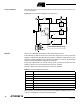
Table 22. DDCn Effects on Port C Pins
DDCn PORTCn I/O Pull-up Comment
0 0 Input No Tri-state (high-Z)
0 1 Input Yes PCn will source current if ext. pulled low.
1 0 Output No Push-pull Zero Output
1 1 Output No Push-pull One Output