
Specifications


59
AT90S8515
0841G–09/01
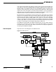
Analog Comparator The Analog Comparator compares the input values on the positive input PB2 (AIN0) and
negative input PB3 (AIN1). When the voltage on the positive input PB2 (AIN0) is higher
than the voltage on the negative input PB3 (AIN1), the Analog Comparator Output
(ACO) is set (one). The comparator’s output can be set to trigger the Timer/Counter1
Input Capture function. In addition, the comparator can trigger a separate interrupt,
exclusive to the Analog Comparator. The user can select interrupt triggering on compar-
ator output rise, fall or toggle. A block diagram of the comparator and its surrounding
logic is shown in Figure 41
.
Figure 41. Analog Comparator Block Diagram
Analog Comparator Control
and Status Register – ACSR
• Bit 7 – ACD: Analog Comparator Disable
When this bit is set (one), the power to the Analog Comparator is switched off. This bit
can be set at any time to turn off the Analog Comparator. This will reduce power con-
sumption in active and idle mode. When changing the ACD bit, the Analog Comparator
interrupt must be disabled by clearing the ACIE bit in ACSR. Otherwise an interrupt can
occur when the bit is changed.
• Bit 6 – Res: Reserved Bit
This bit is a reserved bit in the AT90S8515 and will always read as zero.
• Bit 5 – ACO: Analog Comparator Output
ACO is directly connected to the comparator output.
• Bit 4 – ACI: Analog Comparator Interrupt Flag
This bit is set (one) when a comparator output event triggers the interrupt mode defined
by ACI1 and ACI0. The Analog Comparator Interrupt routine is executed if the ACIE bit
is set (one) and the I-bit in SREG is set (one). ACI is cleared by hardware when execut-
ing the corresponding interrupt handling vector. Alternatively, ACI is cleared by writing a
logical “1” to the flag. Observe however, that if another bit in this register is modified
Bit 76543210
$08 ($28) ACD – ACO ACI ACIE ACIC ACIS1 ACIS0 ACSR
Read/Write R/W R R R/W R/W R/W R/W R/W
Initial Value 0 0 N/A 0 0 0 0 0