
Specifications


36
AT90S8515
0841G–09/01
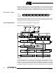
Timer/Counter1 Control
Register A – TCCR1A
• Bits 7, 6 – COM1A1, COM1A0: Compare Output Mode1A, Bits 1 and 0
The COM1A1 and COM1A0 control bits determine any output pin action following a
compare match in Timer/Counter1. Any output pin actions affect pin OC1A (Output
CompareA pin 1). This is an alternative function to an I/O port and the
corresponding direction control bit must be set (one) to control the output pin. The con-
trol configuration is shown in Table 8.
• Bits 5, 4 – COM1B1, COM1B0: Compare Output Mode1B, Bits 1 and 0
The COM1B1 and COM1B0 control bits determine any output pin action following a
compare match in Timer/Counter1. Any output pin actions affect pin OC1B (Output
CompareB). The control configuration is given in Table 8.
Note: X = A or B
In PWM mode, these bits have a different function. Refer to Table 12 on page 40 for a
detailed description.
• Bits 3..2 – Res: Reserved Bits
These bits are reserved bits in the AT90S8515 and always read zero.
• Bits 1..0 – PWM11, PWM10: Pulse Width Modulator Select Bits 1 and 0
These bits select PWM operation of Timer/Counter1 as specified in Table 9. This mode
is described on page 40.
Bit 7 6 5 4 3 2 1 0
$2F ($4F)
COM1A1 COM1A0 COM1B1 COM1B0 – – PWM11 PWM10 TCCR1A
Read/Write R/W R/W R/W R/W R R R/W R/W
Initial Value 0 0 0 0 0 0 0 0
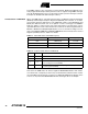
Table 8. Compare 1 Mode Select
COM1X1 COM1X0 Description
0 0 Timer/Counter1 disconnected from output pin OC1X
0 1 Toggle the OC1X output line.
1 0 Clear the OC1X output line (to zero).
1 1 Set the OC1X output line (to one).
Table 9. PWM Mode Select
PWM11 PWM10 Description
0 0 PWM operation of Timer/Counter1 is disabled
0 1 Timer/Counter1 is an 8-bit PWM
1 0 Timer/Counter1 is a 9-bit PWM
1 1 Timer/Counter1 is a 10-bit PWM