Features • Utilizes the AVR® RISC Architecture • AVR – High-performance and Low-power RISC Architecture • • • • • • • • – 118 Powerful Instructions – Most Single Clock Cycle Execution – 32 x 8 General-purpose Working Registers – Up to 8 MIPS Throughput at 8 MHz Data and Nonvolatile Program Memory – 8K Bytes of In-System Programmable Flash Endurance: 1,000 Write/Erase Cycles – 512 Bytes of SRAM – 512 Bytes of In-System Programmable EEPROM Endurance: 100,000 Write/Erase Cycles – Programming Lock for Flas
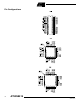
Pin Configurations 2 AT90S8515 0841G–09/01
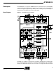
AT90S8515 Description The AT90S8515 is a low-power CMOS 8-bit microcontroller based on the AVR RISC architecture. By executing powerful instructions in a single clock cycle, the AT90S8515 achieves throughputs approaching 1 MIPS per MHz, allowing the system designer to optimize power consumption versus processing speed. Block Diagram Figure 1. The AT90S8515 Block Diagram The AVR core combines a rich instruction set with 32 general-purpose working registers.
one clock cycle. The resulting architecture is more code efficient while achieving throughputs up to ten times faster than conventional CISC microcontrollers.
AT90S8515 current if the pull-up resistors are activated. The Port D pins are tri-stated when a reset condition becomes active, even if the clock is not active. Port D also serves the functions of various special features of the AT90S8515 as listed on page 73. RESET Reset input. A low level on this pin for more than 50 ns will generate a reset, even if the clock is not running. Shorter pulses are not guaranteed to generate a reset.
Crystal Oscillator XTAL1 and XTAL2 are input and output, respectively, of an inverting amplifier that can be configured for use as an on-chip oscillator, as shown in Figure 2. Either a quartz crystal or a ceramic resonator may be used. To drive the device from an external clock source, XTAL2 should be left unconnected while XTAL1 is driven as shown in Figure 3. Figure 2.
AT90S8515 Architectural Overview The fast-access register file concept contains 32 x 8-bit general-purpose working registers with a single clock cycle access time. This means that during one single clock cycle, one ALU (Arithmetic Logic Unit) operation is executed. Two operands are output from the register file, the operation is executed and the result is stored back in the register file – in one clock cycle.
Figure 4.
AT90S8515 Figure 5. Memory Maps Program Memory Data Memory $000 32 Gen.
General-purpose Register File Figure 6 shows the structure of the 32 general-purpose working registers in the CPU. Figure 6. AVR CPU General-purpose Working Registers 7 0 Addr.
AT90S8515 In the different addressing modes these address registers have functions as fixed displacement, automatic increment and decrement (see the descriptions for the different instructions). ALU – Arithmetic Logic Unit The high-performance AVR ALU operates in direct connection with all the 32 generalpurpose working registers. Within a single clock cycle, ALU operations between registers in the register file are executed.
SRAM Data Memory – Internal and External Figure 8 shows how the AT90S8515 SRAM memory is organized. Figure 8.
AT90S8515 two additional clock cycles is used per byte. This has the following effect: Data transfer instructions take two extra clock cycles, whereas interrupt, subroutine calls and returns will need four clock cycles more than specified in the instruction set manual. The five different addressing modes for the data memory cover: Direct, Indirect with Displacement, Indirect, Indirect with Pre-decrement and Indirect with Post-increment.
Register Direct, Two Registers Rd and Rr Figure 10. Direct Register Addressing, Two Registers Operands are contained in register r (Rr) and d (Rd). The result is stored in register d (Rd). I/O Direct Figure 11. I/O Direct Addressing Operand address is contained in six bits of the instruction word. n is the destination or source register address. Data Direct 14 Figure 12.
AT90S8515 A 16-bit data address is contained in the 16 LSBs of a 2-word instruction. Rd/Rr specify the destination or source register. Data Indirect with Displacement Figure 13. Data Indirect with Displacement Operand address is the result of the Y- or Z-register contents added to the address contained in six bits of the instruction word. Data Indirect Figure 14. Data Indirect Addressing Operand address is the contents of the X-, Y-, or the Z-register. Data Indirect with Predecrement Figure 15.
The X-, Y-, or the Z-register is decremented before the operation. Operand address is the decremented contents of the X-, Y-, or the Z-register. Data Indirect with Postincrement Figure 16. Data Indirect Addressing with Post-increment The X-, Y-, or the Z-register is incremented after the operation. Operand address is the content of the X-, Y-, or the Z-register prior to incrementing. Constant Addressing Using the LPM Instruction Figure 17.
AT90S8515 Indirect Program Addressing, IJMP and ICALL Figure 18. Indirect Program Memory Addressing PROGRAM MEMORY $000 15 0 Z-REGISTER $FFF Program execution continues at address contained by the Z-register (i.e., the PC is loaded with the contents of the Z-register). Relative Program Addressing, RJMP and RCALL Figure 19. Relative Program Memory Addressing PROGRAM MEMORY $000 15 0 PC +1 15 12 11 OP 0 k $FFF Program execution continues at address PC + k + 1.
Figure 20. The Parallel Instruction Fetches and Instruction Executions T1 T2 T3 T4 System Clock Ø 1st Instruction Fetch 1st Instruction Execute 2nd Instruction Fetch 2nd Instruction Execute 3rd Instruction Fetch 3rd Instruction Execute 4th Instruction Fetch Figure 21 shows the internal timing concept for the register file. In a single clock cycle an ALU operation using two register operands is executed and the result is stored back to the destination register. Figure 21.
AT90S8515 I/O Memory The I/O space definition of the AT90S8515 is shown in Table 1. Table 1.
Table 1.
AT90S8515 into T by the BST instruction and a bit in T can be copied into a bit in a register in the register file by the BLD instruction. • Bit 5 – H: Half-carry Flag The half-carry flag H indicates a half-carry in some arithmetic operations. See the Instruction Set description for detailed information. • Bit 4 – S: Sign Bit, S = N⊄⊕ V The S-bit is always an exclusive or between the negative flag N and the two’s complement overflow flag V. See the Instruction Set description for detailed information.
Reset and Interrupt Handling The AT90S8515 provides 12 different interrupt sources. These interrupts and the separate reset vector each have a separate program vector in the program memory space. All interrupts are assigned individual enable bits that must be set (one) together with the I-bit in the Status Register in order to enable the interrupt. The lowest addresses in the program memory space are automatically defined as the Reset and Interrupt vectors. The complete list of vectors is shown in Table 2.
AT90S8515 $00f ldi r16,low(RAMEND) $010 out SPL,r16 $011 … Reset Sources … … xxx … The AT90S8515 has three sources of reset: • Power-on Reset. The MCU is reset when the supply voltage is below the Power-on Reset threshold (VPOT). • External Reset. The MCU is reset when a low level is present on the RESET pin for more than 50 ns. • Watchdog Reset. The MCU is reset when the Watchdog timer period expires and the Watchdog is enabled.
The user can select the start-up time according to typical oscillator start-up. The number of WDT oscillator cycles used for each time-out is shown in Table 4. The frequency of the Watchdog Oscillator is voltage-dependent as shown in “Typical Characteristics” on page 95. Table 4. Number of Watchdog Oscillator Cycles Power-on Reset FSTRT Time-out at VCC = 5V Number of WDT Cycles Programmed 0.28 ms 256 Unprogrammed 16.
AT90S8515 External Reset An external reset is generated by a low level on the RESET pin. Reset pulses longer than 50 ns will generate a reset, even if the clock is not running. Shorter pulses are not guaranteed to generate a reset. When the applied signal reaches the Reset Threshold Voltage (VRST) on its positive edge, the delay timer starts the MCU after the Time-out period tTOUT has expired. Figure 26.
interrupt. Some of the interrupt flags can also be cleared by writing a logical “1” to the flag bit position(s) to be cleared. If an interrupt condition occurs when the corresponding interrupt enable bit is cleared (zero), the interrupt flag will be set and remembered until the interrupt is enabled or the flag is cleared by software.
AT90S8515 • Bit 6 – INTF0: External Interrupt Flag0 When an edge on the INT0 pin triggers an interrupt request, the corresponding interrupt flag, INTF0, becomes set (one). If the I-bit in SREG and the corresponding interrupt enable bit, INT0 in GIMSK are set (one), the MCU will jump to the interrupt vector. The flag is cleared when the interrupt routine is executed. Alternatively, the flag is cleared by writing a logical “1” to it. This flag is always cleared when INT0 is configured as level interrupt.
Timer/Counter Interrupt Flag Register – TIFR Bit 7 6 5 4 3 2 1 TOV1 OCF1A OCIFB – ICF1 – TOV0 – Read/Write R/W R/W R/W R R/W R R/W R Initial Value 0 0 0 0 0 0 0 0 $38 ($58) 0 TIFR • Bit 7 – TOV1: Timer/Counter1 Overflow Flag The TOV1 is set (one) when an overflow occurs in Timer/Counter1. TOV1 is cleared by hardware when executing the corresponding interrupt handling vector. Alternatively, TOV1 is cleared by writing a logical “1” to the flag.
AT90S8515 External Interrupts The external interrupts are triggered by the INT1 and INT0 pins. Observe that, if enabled, the interrupts will trigger even if the INT0/INT1 pins are configured as outputs. This feature provides a way of generating a software interrupt. The external interrupts can be triggered by a falling or rising edge or a low level. This is set up as indicated in the specification for the MCU Control Register (MCUCR).
• Bit 5 – SE: Sleep Enable The SE bit must be set (one) to make the MCU enter the Sleep Mode when the SLEEP instruction is executed. To avoid the MCU entering the Sleep Mode, unless it is the programmer’s purpose, it is recommended to set the Sleep Enable (SE) bit just before the execution of the SLEEP instruction. • Bit 4 – SM: Sleep Mode This bit selects between the two available sleep modes. When SM is cleared (zero), Idle Mode is selected as Sleep Mode.
AT90S8515 Sleep Modes To enter the sleep modes, the SE bit in MCUCR must be set (one) and a SLEEP instruction must be executed. If an enabled interrupt occurs while the MCU is in a sleep mode, the MCU awakes, executes the interrupt routine and resumes execution from the instruction following SLEEP. The contents of the register file, SRAM and I/O memory are unaltered. If a reset occurs during Sleep Mode, the MCU wakes up and executes from the Reset vector.
Timer/Counters The AT90S8515 provides two general-purpose Timer/Counters – one 8-bit T/C and one 16-bit T/C. The Timer/Counters have individual prescaling selection from the same 10bit prescaling timer. Both Timer/Counters can either be used as a timer with an internal clock time base or as a counter with an external pin connection that triggers the counting. Timer/Counter Prescaler Figure 28 shows the general Timer/Counter prescaler. Figure 28.
AT90S8515 Figure 29. Timer/Counter0 Block Diagram Timer/Counter0 Control Register – TCCR0 Bit 7 6 5 4 3 2 1 0 $33 ($53) – – – – – CS02 CS01 CS00 Read/Write R R R R R R/W R/W R/W Initial Value 0 0 0 0 0 0 0 0 TCCR0 • Bits 7..3 – Res: Reserved Bits These bits are reserved bits in the AT90S8515 and always read as zero. • Bits 2, 1, 0 – CS02, CS01, CS00: Clock Select0, Bits 2, 1 and 0 The Clock Select0 bits 2, 1 and 0 define the prescaling source of Timer/Counter0.
The Stop condition provides a Timer Enable/Disable function. The CK down divided modes are scaled directly from the CK oscillator clock. If the external pin modes are used for Timer/Counter0, transitions on PB0/(T0) will clock the counter even if the pin is configured as an output. This feature can give the user software control of the counting.
AT90S8515 (TCCR1A and TCCR1B). The interrupt enable/disable settings for Timer/Counter1 are found in the Timer/Counter Interrupt Mask Register (TIMSK). When Timer/Counter1 is externally clocked, the external signal is synchronized with the oscillator frequency of the CPU. To assure proper sampling of the external clock, the minimum time between two external clock transitions must be at least one internal CPU clock period. The external clock signal is sampled on the rising edge of the internal CPU clock.
Timer/Counter1 Control Register A – TCCR1A Bit 7 6 5 4 3 2 1 0 COM1A1 COM1A0 COM1B1 COM1B0 – – PWM11 PWM10 Read/Write R/W R/W R/W R/W R R R/W R/W Initial Value 0 0 0 0 0 0 0 0 $2F ($4F) TCCR1A • Bits 7, 6 – COM1A1, COM1A0: Compare Output Mode1A, Bits 1 and 0 The COM1A1 and COM1A0 control bits determine any output pin action following a compare match in Timer/Counter1. Any output pin actions affect pin OC1A (Output CompareA pin 1).
AT90S8515 Timer/Counter1 Control Register B – TCCR1B Bit 7 6 5 4 3 2 1 0 $2E ($4E) ICNC1 ICES1 – – CTC1 CS12 CS11 CS10 Read/Write R/W R/W R R R/W R/W R/W R/W Initial Value 0 0 0 0 0 0 0 0 TCCR1B • Bit 7 – ICNC1: Input Capture1 Noise Canceler (4 CKs) When the ICNC1 bit is cleared (zero), the input capture trigger noise canceler function is disabled. The input capture is triggered at the first rising/falling edge sampled on the ICP (input capture pin) as specified.
The Stop condition provides a Timer Enable/Disable function. The CK down divided modes are scaled directly from the CK oscillator clock. If the external pin modes are used for Timer/Counter1, transitions on PB1/(T1) will clock the counter even if the pin is configured as an output. This feature can give the user software control of the counting.
AT90S8515 Timer/Counter1 Output Compare Register – OCR1BH AND OCR1BL Bit $29 ($49) 15 14 13 12 11 10 9 OCR1BH $28 ($48) Read/Write Initial Value 8 MSB LSB 7 6 5 4 3 2 1 0 R/W R/W R/W R/W R/W R/W R/W R/W R/W R/W R/W R/W R/W R/W R/W R/W 0 0 0 0 0 0 0 0 0 0 0 0 0 0 0 0 OCR1BL The output compare registers are 16-bit read/write registers. The Timer/Counter1 Output Compare registers contain the data to be continuously compared with Timer/Counter1.
The TEMP register is also used when accessing TCNT1, OCR1A and OCR1B. If the main program and interrupt routines perform access to registers using TEMP, interrupts must be disabled during access from the main program (and from interrupt routines if interrupts are allowed from within interrupt routines).
AT90S8515 Figure 32. Effects on Unsynchronized OCR1 Latching Compare Value changes Counter Value Compare Value PWM Output OC1X Synchronized OCR1X Latch Compare Value changes Counter Value Compare Value PWM Output OC1X Unsynchronized OCR1X Latch Glitch Note: X = A or B During the time between the write and the latch operation, a read from OCR1A or OCR1B will read the contents of the temporary location. This means that the most recently written value always will read out of OCR1A/B.
Watchdog Timer The Watchdog Timer is clocked from a separate On-chip oscillator that runs at 1 MHz. This is the typical value at VCC = 5V. See characterization data for typical values at other VCC levels. By controlling the Watchdog Timer prescaler, the Watchdog reset interval can be adjusted (see Table 14 for a detailed description). The WDR (Watchdog Reset) instruction resets the Watchdog Timer. Eight different clock cycle periods can be selected to determine the reset period.
AT90S8515 1. In the same operation, write a logical “1” to WDTOE and WDE. A logical “1” must be written to WDE even though it is set to one before the disable operation starts. 2. Within the next four clock cycles, write a logical “0” to WDE. This disables the Watchdog. • Bits 2..0 – WDP2, WDP1, WDP0: Watchdog Timer Prescaler 2, 1 and 0 The WDP2, WDP1 and WDP0 bits determine the Watchdog Timer prescaling when the Watchdog Timer is enabled.
EEPROM Read/Write Access The EEPROM access registers are accessible in the I/O space. The write access time is in the range of 2.5 - 4 ms, depending on the VCC voltages. A self-timing function, however, lets the user software detect when the next byte can be written. If the user code contains code that writes the EEPROM, some precaution must be taken. In heavily filtered power supplies, VCC is likely to rise or fall slowly on powerup/down.
AT90S8515 • Bit 2 – EEMWE: EEPROM Master Write Enable The EEMWE bit determines whether setting EEWE to one causes the EEPROM to be written. When EEMWE is set (one), setting EEWE will write data to the EEPROM at the selected address. If EEMWE is zero, setting EEWE will have no effect. When EEMWE has been set (one) by software, hardware clears the bit to zero after four clock cycles. See the description of the EEWE bit for a EEPROM write procedure.
Prevent EEPROM Corruption During periods of low VCC, the EEPROM data can be corrupted because the supply voltage is too low for the CPU and the EEPROM to operate properly. These issues are the same as for board level systems using the EEPROM and the same design solutions should be applied. An EEPROM data corruption can be caused by two situations when the voltage is too low. First, a regular write sequence to the EEPROM requires a minimum voltage to operate correctly.
AT90S8515 Serial Peripheral Interface – SPI The Serial Peripheral Interface (SPI) allows high-speed synchronous data transfer between the AT90S8515 and peripheral devices or between several AVR devices.
Figure 35. SPI Master-slave Interconnection MSB MASTER LSB MISO MISO 8-BIT SHIFT REGISTER MSB SLAVE LSB 8-BIT SHIFT REGISTER MOSI MOSI SPI CLOCK GENERATOR SCK SS SCK SS VCC The system is single-buffered in the transmit direction and double-buffered in the receive direction. This means that bytes to be transmitted cannot be written to the SPI Data Register before the entire shift cycle is completed.
AT90S8515 pins are inputs. When SS is driven high, all pins are inputs and the SPI is passive, which means that it will not receive incoming data. Note that the SPI logic will be reset once the SS pin is brought high. If the SS pin is brought high during a transmission, the SPI will stop sending and receiving immediately and both data received and data sent must be considered as lost.
• Bit 5 – DORD: Data Order When the DORD bit is set (one), the LSB of the data word is transmitted first. When the DORD bit is cleared (zero), the MSB of the data word is transmitted first. • Bit 4 – MSTR: Master/Slave Select This bit selects Master SPI Mode when set (one), and Slave SPI Mode when cleared (zero). If SS is configured as an input and is driven low while MSTR is set, MSTR will be cleared and SPIF in SPSR will become set. The user will then have to set MSTR to reenable SPI Master Mode.
AT90S8515 SPI Data Register – SPDR Bit 7 6 5 4 3 2 1 0 $0F ($2F) MSB LSB Read/Write R/W R/W R/W R/W R/W R/W R/W R/W Initial Value x x x x x x x x SPDR Undefined The SPI Data Register is a read/write register used for data transfer between the register file and the SPI Shift Register. Writing to the register initiates data transmission. Reading the register causes the Shift Register Receive buffer to be read.
UART The AT90S8515 features a full duplex (separate receive and transmit registers) Universal Asynchronous Receiver and Transmitter (UART).
AT90S8515 If the 10(11)-bit Transmitter shift register is empty, data is transferred from UDR to the shift register. At this time the UDRE (UART Data Register Empty) bit in the UART Status Register, USR, is set. When this bit is set (one), the UART is ready to receive the next character. At the same time as the data is transferred from UDR to the 10(11)-bit shift register, bit 0 of the shift register is cleared (start bit) and bit 9 or 10 is set (stop bit).
The receiver front-end logic samples the signal on the RXD pin at a frequency 16 times the baud rate. While the line is idle, one single sample of logical “0” will be interpreted as the falling edge of a start bit and the start bit detection sequence is initiated. Let sample 1 denote the first zero-sample. Following the 1-to-0 transition, the receiver samples the RXD pin at samples 8, 9 and 10.
AT90S8515 UART Control UART I/O Data Register – UDR Bit 7 6 5 4 3 2 1 0 $0C ($2C) MSB LSB Read/Write R/W R/W R/W R/W R/W R/W R/W R/W Initial Value 0 0 0 0 0 0 0 0 UDR The UDR register is actually two physically separate registers sharing the same I/O address. When writing to the register, the UART Transmit Data register is written. When reading from UDR, the UART Receive Data register is read.
The FE bit is cleared when the stop bit of received data is one. • Bit 3 – OR: Overrun This bit is set if an Overrun condition is detected, i.e., when a character already present in the UDR register is not read before the next character has been shifted into the Receiver Shift register. The OR bit is buffered, which means that it will be set once the valid data still in UDRE is read. The OR bit is cleared (zero) when data is received and transferred to UDR. • Bits 2..
AT90S8515 BAUD Rate Generator The baud rate generator is a frequency divider that generates baud rates according to the following equation: f CK BAUD = -----------------------------------16(UBRR + 1) • BAUD = Baud rate • fCK = Crystal Clock frequency • UBRR = Contents of the UART Baud Rate register, UBRR (0 - 255) For standard crystal frequencies, the most commonly used baud rates can be generated by using the UBRR settings in Table 17.
Table 17. UBRR Settings at Various Crystal Frequencies Baud Rate 1 MHz %Error 1.8432 MHz %Error 2 MHz %Error 2.4576 MHz %Error 2400 UBRR= 25 0.2 UBRR= 47 0.0 UBRR= 51 0.2 UBRR= 63 0.0 4800 UBRR= 12 0.2 UBRR= 23 0.0 UBRR= 25 0.2 UBRR= 31 0.0 6 7.5 UBRR= 9600 UBRR= 11 0.0 UBRR= 12 0.2 UBRR= 15 0.0 3 7.8 UBRR= 8 3.7 UBRR= 10 3.1 14400 UBRR= 7 0.0 UBRR= 2 7.8 UBRR= 6 7.5 UBRR= 19200 UBRR= 5 0.0 UBRR= 7 0.0 1 7.8 UBRR= 3 7.8 UBRR= 4 6.3 28800 UBRR= 3 0.0 UBRR= UBRR= 1 22.9 UBRR= UBRR= 2 7.8 UBRR= 38400 2 0.
AT90S8515 Analog Comparator The Analog Comparator compares the input values on the positive input PB2 (AIN0) and negative input PB3 (AIN1). When the voltage on the positive input PB2 (AIN0) is higher than the voltage on the negative input PB3 (AIN1), the Analog Comparator Output (ACO) is set (one). The comparator’s output can be set to trigger the Timer/Counter1 Input Capture function. In addition, the comparator can trigger a separate interrupt, exclusive to the Analog Comparator.
using the SBI or CBI instruction, ACI will be cleared if it has become set before the operation. • Bit 3 – ACIE: Analog Comparator Interrupt Enable When the ACIE bit is set (one) and the I-bit in the Status Register is set (one), the Analog Comparator interrupt is activated. When cleared (zero), the interrupt is disabled. • Bit 2 – ACIC: Analog Comparator Input Capture Enable When set (one), this bit enables the Input Capture function in Timer/Counter1 to be triggered by the Analog Comparator.
AT90S8515 Default, the external SRAM access, is a 3-cycle scheme as depicted in Figure 43. When one extra wait state is needed in the access cycle, set the SRW bit (one) in the MCUCR register. The resulting access scheme is shown in Figure 44. In both cases, note that PORTA is data bus in one cycle only. As soon as the data access finishes, PORTA becomes a low-order address bus again.
Figure 44. External Data SRAM Memory Cycles with Wait State T1 T2 T3 T4 System Clock Ø ALE Prev. Address Address Address Data Addr. Write Data/Address [7..0] Prev. Address Addr. Read Address [15..8] WR Data/Address [7..0] Prev.
AT90S8515 I/O Ports All AVR ports have true read-modify-write functionality when used as general digital I/O ports. This means that the direction of one port pin can be changed without unintentionally changing the direction of any other pin with the SBI and CBI instructions. The same applies for changing drive value (if configured as output) or the enabling/disabling of pull-up resistors (if configured as input). Port A Port A is an 8-bit bi-directional I/O port.
PORTAn has to be cleared (zero) or the pin has to be configured as an output pin. The Port A pins are tri-stated when a reset condition becomes active, even if the clock is not active.. Table 19. DDAn Effects on Port A Pins DDAn PORTAn I/O Pull-up 0 0 Input No Tri-state (high-Z) 0 1 Input Yes PAn will source current if ext. pulled low. 1 0 Output No Push-pull Zero Output 1 1 Output No Push-pull One Output Note: Port A Schematics Comment n: 7,6…0, pin number.
AT90S8515 Port B Port B is an 8-bit bi-directional I/O port. Three I/O memory address locations are allocated for the Port B, one each for the Data Register – PORTB, $18($38), Data Direction Register – DDRB, $17($37) and the Port B Input Pins – PINB, $16($36). The Port B Input Pins address is read-only, while the Data Register and the Data Direction Register are read/write. All port pins have individually selectable pull-up resistors.
Port B as General Digital I/O All eight pins in Port B have equal functionality when used as digital I/O pins. PBn, general I/O pin: The DDBn bit in the DDRB register selects the direction of this pin. If DDBn is set (one), PBn is configured as an output pin. If DDBn is cleared (zero), PBn is configured as an input pin. If PORTBn is set (one) when the pin is configured as an input pin, the MOS pull-up resistor is activated.
AT90S8515 • AIN0 – Port B, Bit 2 AIN0: Analog Comparator Positive Input. When configured as an input (DDB2 is cleared [zero]) and with the internal MOS pull-up resistor switched off (PB2 is cleared [zero]), this pin also serves as the positive input of the On-chip Analog Comparator. • T1 – Port B, Bit 1 T1: Timer/Counter1 counter source. See the timer description for further details • T0 – Port B, Bit 0 T0: Timer/Counter0 counter source. See the timer description for further details.
Figure 47. Port B Schematic Diagram (Pins PB2 and PB3) Figure 48.
AT90S8515 Figure 49. Port B Schematic Diagram (Pin PB5) RD MOS PULLUP RESET R Q D DDB5 C DATA BUS WD RESET R Q D PORTB5 PB5 C RL WP RP WP: WD: RL: RP: RD: SPE: MSTR WRITE PORTB WRITE DDRB READ PORTB LATCH READ PORTB PIN READ DDRB SPI ENABLE MASTER SELECT MSTR SPE SPI MASTER OUT SPI SLAVE IN Figure 50.
Figure 51. Port B Schematic Diagram (Pin PB7) RD MOS PULLUP RESET Q R D DDB7 C DATA BUS WD RESET R Q D PORTB7 PB7 C RL WP RP WP: WD: RL: RP: RD: SPE: MSTR WRITE PORTB WRITE DDRB READ PORTB LATCH READ PORTB PIN READ DDRB SPI ENABLE MASTER SELECT MSTR SPE SPI CLOCK OUT SPI CLOCK IN Port C Port C is an 8-bit bi-directional I/O port.
AT90S8515 Port C Data Direction Register – DDRC Bit 7 6 5 4 3 2 1 0 DDC7 DDC6 DDC5 DDC4 DDC3 DDC2 DDC1 DDC0 Read/Write R/W R/W R/W R/W R/W R/W R/W R/W Initial Value 0 0 0 0 0 0 0 0 $14 ($34) Port C Input Pins Address – PINC Bit 7 6 5 4 3 2 1 0 PINC7 PINC6 PINC5 PINC4 PINC3 PINC2 PINC1 PINC0 Read/Write R R R R R R R R Initial Value N/A N/A N/A N/A N/A N/A N/A N/A $13 ($33) DDRC PINC The Port C Input Pins address (PINC) is not a regis
Port C Schematics Note that all port pins are synchronized. The synchronization latch is, however, not shown in the figure. Figure 52. Port C Schematic Diagram (Pins PC0 - PC7) Port D Port D is an 8-bit bi-directional I/O port with internal pull-up resistors. Three I/O memory address locations are allocated for the Port D, one each for the Data Register – PORTD, $12($32), Data Direction Register – DDRD, $11($31) and the Port D Input Pins – PIND, $10($30).
AT90S8515 Port D Data Register – PORTD Bit 7 6 5 4 3 2 1 0 PORTD7 PORTD6 PORTD5 PORTD4 PORTD3 PORTD2 PORTD1 PORTD0 Read/Write R/W R/W R/W R/W R/W R/W R/W R/W Initial Value 0 0 0 0 0 0 0 0 $12 ($32) Port D Data Direction Register – DDRD Bit 7 6 5 4 3 2 1 0 DDD7 DDD6 DDD5 DDD4 DDD3 DDD2 DDD1 DDD0 Read/Write R/W R/W R/W R/W R/W R/W R/W R/W Initial Value 0 0 0 0 0 0 0 0 $11 ($31) Port D Input Pins Address – PIND Bit 7 6 5 4 3 2 1
• INT1 – Port D, Bit 3 INT1: External Interrupt source 1. The PD3 pin can serve as an external interrupt source to the MCU. See the interrupt description for further details and how to enable the source. • INT0 – Port D, Bit 2 INT0: External Interrupt source 0. The PD2 pin can serve as an external interrupt source to the MCU. See the interrupt description for further details and how to enable the source. • TXD – Port D, Bit 1 Transmit Data (data output pin for the UART).
AT90S8515 Figure 54. Port D Schematic Diagram (Pin PD1) RD MOS PULLUP RESET Q R D DDD1 C DATA BUS WD RESET R Q D PORTD1 PD1 C RL WP RP WP: WD: RL: RP: RD: TXD: TXEN: WRITE PORTD WRITE DDRD READ PORTD LATCH READ PORTD PIN READ DDRD UART TRANSMIT DATA UART TRANSMIT ENABLE TXEN TXD Figure 55.
Figure 56. Port D Schematic Diagram (Pin PD4) Figure 57.
AT90S8515 Figure 58. Port D Schematic Diagram (Pin PD6) Figure 59.
Memory Programming Program and Data Memory Lock Bits The AT90S8515 MCU provides two Lock bits that can be left unprogrammed (“1”) or can be programmed (“0”) to obtain the additional features listed in Table 25. The Lock bits can only be erased with the Chip Erase command. Table 25. Lock Bit Protection Modes Memory Lock Bits Mode LB1 LB2 1 1 1 No memory lock features enabled. 2 0 1 Further programming of the Flash and EEPROM is disabled.(1) 3 0 0 Same as mode 2, and verify is also disabled.
AT90S8515 the self-timed write operation in the serial programming mode. During programming, the supply voltage must be in accordance with Table 26. Table 26. Supply Voltage during Programming Part Serial Programming Parallel Programming AT90S8515 2.7 - 6.0V 4.5 - 5.5V Parallel Programming This section describes how to parallel program and verify Flash program memory, EEPROM data memory, Lock bits and Fuse bits in the AT90S8515.
Table 27. Pin Name Mapping Signal Name in Programming Mode Pin Name I/O Function RDY/BSY PD1 O 0: Device is busy programming, 1: Device is ready for new command OE PD2 I Output Enable (Active low) WR PD3 I Write Pulse (Active low) BS PD4 I Byte Select (“0” selects low byte, “1” selects high byte) XA0 PD5 I XTAL Action Bit 0 XA1 PD6 I XTAL Action Bit 1 DATA PB7-0 I/O Bi-directional Data Bus (Output when OE is low) Table 28.
AT90S8515 Chip Erase The Chip Erase command will erase the Flash and EEPROM memories and the Lock bits. The Lock bits are not reset until the Flash and EEPROM have been completely erased. The Fuse bits are not changed. Chip Erase must be performed before the Flash or EEPROM is reprogrammed. Load Command “Chip Erase” 1. Set XA1, XA0 to “10”. This enables command loading. 2. Set BS to “0”. 3. Set DATA to “1000 0000”. This is the command for Chip Erase. 4. Give XTAL1 a positive pulse. This loads the command.
1. Set BS to “1”. This selects high data. 2. Give WR a negative pulse. This starts programming of the data byte. RDY/BSY goes low. 3. Wait until RDY/BSY goes high to program the next byte. (See Figure 62 for signal waveforms.) The loaded command and address are retained in the device during programming. For efficient programming, the following should be considered: • The command needs only be loaded once when writing or reading multiple memory locations.
AT90S8515 Figure 62. Programming the Flash Waveforms (Continued) DATA DATA HIGH XA1 XA0 BS XTAL1 WR RDY/BSY RESET +12V OE Reading the Flash The algorithm for reading the Flash memory is as follows (refer to “Programming the Flash” for details on command and address loading): 1. A: Load Command “0000 0010”. 2. B: Load Address High Byte ($00 - $0F). 3. C: Load Address Low Byte ($00 - $FF). 4. Set OE to “0”, and BS to “0”. The Flash word low byte can now be read at DATA. 5. Set BS to “1”.
Bit 5 = SPIEN Fuse bit Bit 0 = FSTRT Fuse bit Bit 7 - 6, 4 - 1 = “1”. These bits are reserved and should be left unprogrammed (“1”). 3. Give WR a tWLWH_PFB-wide negative pulse to execute the programming, tWLWH_PFB is found in Table 30. Programming the Fuse bits does not generate any activity on the RDY/BSY pin. Programming the Lock Bits The algorithm for programming the Lock bits is as follows (refer to “Programming the Flash” on page 81 for details on command and data loading): 1.
AT90S8515 Parallel Programming Characteristics Figure 63. Parallel Programming Timing tXLWL tXHXL XTAL1 tDVXH tXLDX tBVWL Data & Control (DATA, XA0/1, BS) Write tWLWH WR tRHBX tWHRL RDY/BSY tWLRH tXLOL tOHDZ tOLDV Read OE DATA Table 30. Parallel Programming Characteristics, TA = 25°C ± 10%, VCC = 5V ± 10% Symbol Parameter Min VPP Programming Enable Voltage 11.5 IPP Programming Enable Current tDVXH Data and Control Setup before XTAL1 High 67.0 ns tXHXL XTAL1 Pulse Width High 67.
Serial Downloading Both the program and data memory arrays can be programmed using the SPI bus while RESET is pulled to GND. The serial interface consists of pins SCK, MOSI (input) and MISO (output). See Figure 64. After RESET is set low, the Programming Enable instruction needs to be executed first before program/erase instructions can be executed. Figure 64. Serial Programming and Verify 2.7 - 6.
AT90S8515 ing the third byte of the Programming Enable instruction. Whether the echo is correct or not, all four bytes of the instruction must be transmitted. If the $53 did not echo back, give SCK a positive pulse and issue a new Programming Enable instruction. If the $53 is not seen within 32 attempts, there is no functional device connected. 4. If a Chip Erase is performed (must be done to erase the Flash), wait tWD_ERASE after the instruction, give RESET a positive pulse and start over from step 2.
Figure 65. Serial Programming Waveforms Table 32. Serial Programming Instruction Set Instruction Format Instruction Programming Enable Chip Erase Read Program Memory Write Program Memory Read EEPROM Memory Write EEPROM Memory Write Lock Bits Byte 1 Byte 2 Byte 3 Byte4 Operation 1010 1100 0101 0011 xxxx xxxx xxxx xxxx Enable serial programming while RESET is low. 1010 1100 100x xxxx xxxx xxxx xxxx xxxx Chip Erase Flash and EEPROM memory arrays.
AT90S8515 Serial Programming Characteristics Figure 66. Serial Programming Timing MOSI SCK tSLSH tSHOX tOVSH tSHSL MISO tSLIV Table 33. Serial Programming Characteristics, TA = -40°C to 85°C, VCC = 2.7V - 6.0V (unless otherwise noted) Symbol Parameter Min 1/tCLCL Oscillator Frequency (VCC = 2.7 - 4.0V) tCLCL Oscillator Period (VCC = 2.7 - 4.0V) 1/tCLCL Oscillator Frequency (VCC = 4.0 - 6.0V) tCLCL Oscillator Period (VCC = 4.0 - 6.0V) tSHSL Typ 0 Max Units 4.0 MHz 250.0 ns 0 8.
Electrical Characteristics Absolute Maximum Ratings* Operating Temperature.................................. -55°C to +125°C *NOTICE: Storage Temperature ..................................... -65°C to +150°C Voltage on Any Pin except RESET with Respect to Ground .............................-1.0V to VCC + 0.5V Voltage on RESET with Respect to Ground ...................................-1.0V to +13.0V Stresses beyond those listed under “Absolute Maximum Ratings” may cause permanent damage to the device.
AT90S8515 Notes: 1. “Max” means the highest value where the pin is guaranteed to be read as low. 2. “Min” means the lowest value where the pin is guaranteed to be read as high. 3. Although each I/O port can sink more than the test conditions (20 mA at VCC = 5V, 10 mA at VCC = 3V) under steady state conditions (non-transient), the following must be observed: 1] The sum of all IOL, for all ports, should not exceed 200 mA. 2] The sum of all IOL, for ports B0 - B7, D0 - D7 and XTAL2, should not exceed 100 mA.
External Clock Drive Waveforms Figure 67. External Clock VIH1 VIL1 Table 36. External Clock Drive VCC = 2.7V to 4.0V VCC = 4.0V to 6.0V Min Max Min Max Units 0 4.0 0 8.0 MHz Symbol Parameter 1/tCLCL Oscillator Frequency tCLCL Clock Period 250.0 125.0 ns tCHCX High Time 100.0 50.0 ns tCLCX Low Time 100.0 50.0 ns tCLCH Rise Time 1.6 0.5 µs tCHCL Fall Time 1.6 0.
AT90S8515 External Data Memory Timing Table 37. External Data Memory Characteristics, 4.0V - 6.0V, No Wait State 8 MHz Oscillator 0 1 Symbol Parameter 1/tCLCL Oscillator Frequency tLHLL ALE Pulse Width Min Max Variable Oscillator Min 0.0 32.5 Max Unit 8.0 MHz (1) ns (1) 0.5 tCLCL - 30.0 2 tAVLL Address Valid A to ALE Low 22.5 0.5 tCLCL - 40.0 ns 3a tLLAX_ST Address Hold after ALE Low, ST/STD/STS Instructions 67.5 0.5 tCLCL + 5.
Table 39. External Data Memory Characteristics, 2.7V - 4.0V, No Wait State 4 MHz Oscillator 0 Symbol Parameter 1/tCLCL Oscillator Frequency Min Max Variable Oscillator Min 0.0 Max Unit 4.0 MHz (1) ns 1 tLHLL ALE Pulse Width 70.0 0.5 tCLCL - 55.0 2 tAVLL Address Valid A to ALE Low 60.0 0.5 tCLCL - 65.0(1) ns 3a tLLAX_ST Address Hold after ALE Low, ST/STD/STS Instructions 130.0 0.5 tCLCL + 5.0(2) ns 3b tLLAX_LD Address Hold after ALE Low, LD/LDD/LDS Instructions 15.0 15.
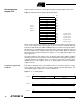
AT90S8515 Typical Characteristics The following charts show typical behavior. These figures are not tested during manufacturing. All current consumption measurements are performed with all I/O pins configured as inputs and with internal pull-ups enabled. ICP is pulled high externally. A sine wave generator with rail-to-rail output is used as clock source. The power consumption in Power-down mode is independent of clock selection.
Figure 70. Active Supply Current vs. VCC ACTIVE SUPPLY CURRENT vs. Vcc FREQUENCY = 4 MHz 14 TA = -40˚C 12 TA = 25˚C 10 I cc(mA) TA = 85˚C 8 6 4 2 0 2 2.5 3 3.5 4 4.5 5 5.5 6 Vcc(V) Figure 71. Idle Supply Current vs. Frequency IDLE SUPPLY CURRENT vs. FREQUENCY TA= 25˚C 12 Vcc= 6V 10 Vcc= 5.5V 8 I cc(mA) Vcc= 5V 6 Vcc= 4.5V Vcc= 4V 4 Vcc= 3.6V Vcc= 3.3V Vcc= 3.0V Vcc= 2.
AT90S8515 Figure 72. Idle Supply Current vs. VCC IDLE SUPPLY CURRENT vs. Vcc FREQUENCY = 4 MHz 4 TA = -40˚C 3.5 TA = 25˚C TA = 85˚C 3 I cc(mA) 2.5 2 1.5 1 0.5 0 2 2.5 3 3.5 4 4.5 5 5.5 6 Vcc(V) Figure 73. Power-down Supply Current vs. VCC POWER DOWN SUPPLY CURRENT vs. Vcc WATCHDOG TIMER DISABLED 12 TA = 85˚C 10 I cc(µΑ) 8 6 TA = 70˚C 4 2 TA = 45˚C TA = 25˚C 0 2 2.5 3 3.5 4 4.5 5 5.
Figure 74. Power-down Supply Current vs. VCC POWER DOWN SUPPLY CURRENT vs. Vcc WATCHDOG TIMER ENABLED 140 120 TA = 85˚C 100 I cc(µΑ) TA = 25˚C 80 60 40 20 0 2 2.5 3 3.5 4 4.5 5 5.5 6 Vcc(V) Figure 75. Analog Comparator Current vs. VCC ANALOG COMPARATOR CURRENT vs. Vcc 0.8 0.7 TA = 25˚C TA = -40˚C 0.6 TA = 85˚C I cc(mA) 0.5 0.4 0.3 0.2 0.1 0 2 2.5 3 3.5 4 4.5 5 5.
AT90S8515 Analog Comparator offset voltage is measured as absolute offset. Figure 76. Analog Comparator Offset Voltage vs. Common Mode Voltage ANALOG COMPARATOR OFFSET VOLTAGE vs. COMMON MODE VOLTAGE Vcc = 5V 18 16 TA = 25˚C Offset Voltage (mV) 14 12 TA = 85˚C 10 8 6 4 2 0 0 0.5 1 1.5 2 2.5 3 3.5 4 4.5 5 Common Mode Voltage (V) Figure 77. Analog Comparator Offset Voltage vs. Common Mode Voltage ANALOG COMPARATOR OFFSET VOLTAGE vs. COMMON MODE VOLTAGE Vcc = 2.
Figure 78. Analog Comparator Input Leakage Current ANALOG COMPARATOR INPUT LEAKAGE CURRENT VCC = 6V TA = 25˚C 60 50 30 I ACLK (nA) 40 20 10 0 -10 0 0.5 1 1.5 2 2.5 3 3.5 4 4.5 5 5.5 6 6.5 7 VIN (V) Figure 79. Watchdog Oscillator Frequency vs. VCC WATCHDOG OSCILLATOR FREQUENCY vs. Vcc 1600 TA = 25˚C 1400 TA = 85˚C F RC (KHz) 1200 1000 800 600 400 200 0 2 2.5 3 3.5 4 4.5 5 5.
AT90S8515 Sink and source capabilities of I/O ports are measured on one pin at a time. Figure 80. Pull-up Resistor Current vs. Input Voltage PULL-UP RESISTOR CURRENT vs. INPUT VOLTAGE Vcc = 5V 120 TA = 25˚C 100 TA = 85˚C I OP (µA) 80 60 40 20 0 0 0.5 1 1.5 2 2.5 VOP (V) 3 3.5 4 4.5 5 Figure 81. Pull-up Resistor Current vs. Input Voltage PULL-UP RESISTOR CURRENT vs. INPUT VOLTAGE Vcc = 2.7V 30 TA = 25˚C 25 TA = 85˚C 15 I OP (µA) 20 10 5 0 0 0.5 1 1.5 2 2.
Figure 82. I/O Pin Sink Current vs. Output Voltage I/O PIN SINK CURRENT vs. OUTPUT VOLTAGE Vcc = 5V 70 TA = 25˚C 60 TA = 85˚C 50 30 I OL (mA) 40 20 10 0 0 0.5 1 1.5 2 2.5 3 VOL (V) Figure 83. I/O Pin Source Current vs. Output Voltage I/O PIN SOURCE CURRENT vs. OUTPUT VOLTAGE Vcc = 5V 20 TA = 25˚C 18 16 TA = 85˚C 14 I OH (mA) 12 10 8 6 4 2 0 0 0.5 1 1.5 2 2.5 3 3.5 4 4.
AT90S8515 Figure 84. I/O Pin Source Current vs. Output Voltage I/O PIN SOURCE CURRENT vs. OUTPUT VOLTAGE Vcc = 2.7V 6 TA = 25˚C 5 TA = 85˚C 3 I OH (mA) 4 2 1 0 0 0.5 1 1.5 2 2.5 3 VOH (V) Figure 85. I/O Pin Input Threshold Voltage vs. VCC I/O PIN INPUT THRESHOLD VOLTAGE vs. Vcc TA = 25˚C 2.5 Threshold Voltage (V) 2 1.5 1 0.5 0 2.7 4.0 5.
Figure 86. I/O Pin Input Hysteresis vs. VCC I/O PIN INPUT HYSTERESIS vs. Vcc TA = 25˚C 0.18 0.16 Input hysteresis (V) 0.14 0.12 0.1 0.08 0.06 0.04 0.02 0 2.7 4.0 5.0 Vcc Figure 87. I/O Pin Sink Current vs. Output Voltage I/O PIN SINK CURRENT vs. OUTPUT VOLTAGE Vcc = 2.7V 25 TA = 25˚C 20 TA = 85˚C 10 I OL (mA) 15 5 0 0 0.5 1 1.
AT90S8515 Register Summary Address Name Bit 7 Bit 6 Bit 5 Bit 4 Bit 3 Bit 2 Bit 1 Bit 0 Page $3F ($5F) $3E ($5E) $3D ($5D) $3C ($5C) $3B ($5B) $3A ($5A) $39 ($59) $38 ($58) $37 ($57) $36 ($56) $35 ($55) $34 ($54) $33 ($53) $32 ($52) ... $2F ($4F) $2E ($4E) $2D ($4D) $2C ($4C) $2B ($4B) $2A ($4A) $29 ($49) $28 ($48) ... $25 ($45) $24 ($44) ...
Instruction Set Summary Mnemonic Operands Description ARITHMETIC AND LOGIC INSTRUCTIONS ADD Rd, Rr Add Two Registers ADC Rd, Rr Add with Carry Two Registers ADIW Rdl, K Add Immediate to Word SUB Rd, Rr Subtract Two Registers SUBI Rd, K Subtract Constant from Register SBC Rd, Rr Subtract with Carry Two Registers SBCI Rd, K Subtract with Carry Constant from Reg.
AT90S8515 Instruction Set Summary (Continued) Mnemonic Operands DATA TRANSFER INSTRUCTIONS MOV Rd, Rr LDI Rd, K LD Rd, X LD Rd, X+ LD Rd, -X LD Rd, Y LD Rd, Y+ LD Rd, -Y LDD Rd, Y+q LD Rd, Z LD Rd, Z+ LD Rd, -Z LDD Rd, Z+q LDS Rd, k ST X, Rr ST X+, Rr ST -X, Rr ST Y, Rr ST Y+, Rr ST -Y, Rr STD Y+q, Rr ST Z, Rr ST Z+, Rr ST -Z, Rr STD Z+q, Rr STS k, Rr LPM IN Rd, P OUT P, Rr PUSH Rr POP Rd BIT AND BIT-TEST INSTRUCTIONS SBI P, b CBI P, b LSL Rd LSR Rd ROL Rd ROR Rd ASR Rd SWAP Rd BSET s BCLR s BST Rr, b BLD
AT90S8515 Ordering Information Speed (MHz) Power Supply Ordering Code Package 4 2.7V - 6.0V AT90S8515-4AC AT90S8515-4JC AT90S8515-4PC 44A 44J 40P6 Commercial (0°C to 70°C) AT90S8515-4AI AT90S8515-4JI AT90S8515-4PI 44A 44J 40P6 Industrial (-40°C to 85°C) AT90S8515-8AC AT90S8515-8JC AT90S8515-8PC 44A 44J 40P6 Commercial (0°C to 70°C) AT90S8515-8AI AT90S8515-8JI AT90S8515-8PI 44A 44J 40P6 Industrial (-40°C to 85°C) 8 Note: 4.0V - 6.
AT90S8515 Packaging Information 44A 44-lead, Thin (1.0mm) Plastic Quad Flat Package (TQFP), 10x10mm body, 2.0mm footprint, 0.8mm pitch. Dimension in Millimeters and (Inches)* JEDEC STANDARD MS-026 ACB 12.25(0.482) SQ 11.75(0.462) PIN 1 ID PIN 1 0.45(0.018) 0.30(0.012) 0.80(0.0315) BSC 10.10(0.394) SQ 9.90(0.386) 1.20(0.047) MAX 0.20(0.008) 0.09(0.004) 0˚~7˚ 0.75(0.030) 0.45(0.018) 0.15(0.006) 0.05(0.002) *Controlling dimension: millimetter REV.
44J 44J, 44-lead, Plastic J-leaded Chip Carrier (PLCC) Dimensions in Milimeters and (Inches)* JEDEC STANDARD MS-018 AC 1.14(0.045) X 45˚ 0.813(0.032) 0.660(0.026) PIN NO. 1 IDENTIFY 1.14(0.045) X 45˚ 16.70(0.656) SQ 16.50(0.650) 17.70(0.695) SQ 17.40(0.685) 1.27(0.050) TYP 12.70(0.500) REF SQ 0.318(0.0125) 0.191(0.0075) 16.00(0.630) SQ 15.00(0.590) 0.533(0.021) 0.330(0.013) 0.50(0.020)MIN 2.11(0.083) 1.57(0.062) 3.05(0.120) 2.29(0.090) 4.57(0.180) 4.19(0.165) 0.51(0.
AT90S8515 40P6 40-lead, Plastic Dual Inline Parkage (PDIP), 0.600" wide Demension in Millimeters and (Inches)* JEDEC STANDARD MS-011 AC 52.71(2.075) 51.94(2.045) PIN 1 13.97(0.550) 13.46(0.530) 48.26(1.900) REF 4.83(0.190)MAX SEATING PLANE 0.38(0.015)MIN 3.56(0.140) 3.05(0.120) 2.54(0.100)BSC 1.65(0.065) 1.27(0.050) 0.56(0.022) 0.38(0.015) 15.88(0.625) 15.24(0.600) 0º ~ 15º REF 0.38(0.015) 0.20(0.008) 17.78(0.700)MAX *Controlling dimension: Inches REV.
Atmel Headquarters Atmel Product Operations Corporate Headquarters Atmel Colorado Springs 2325 Orchard Parkway San Jose, CA 95131 TEL (408) 441-0311 FAX (408) 487-2600 Europe Atmel SarL Route des Arsenaux 41 Casa Postale 80 CH-1705 Fribourg Switzerland TEL (41) 26-426-5555 FAX (41) 26-426-5500 Asia Atmel Asia, Ltd. Room 1219 Chinachem Golden Plaza 77 Mody Road Tsimhatsui East Kowloon Hong Kong TEL (852) 2721-9778 FAX (852) 2722-1369 Japan Atmel Japan K.K. 9F, Tonetsu Shinkawa Bldg.