AT91SAM7L-STK Rev. B Starter Kit ....................................................................................................................
1-2 6414A–ATARM–12-Sep-08 AT91SAM7L-STK Rev.
Table of Contents Section 1 Overview .................................................................................................................... 1-1 1.1 Introduction ........................................................................................................................ 1-1 Section 2 Setting Up the AT91SAM7L-STK Board .................................................................... 2-1 2.1 Electrostatic Warning .................................................................
Table of Contents (Continued) Section 5 Configuration .............................................................................................................. 5-1 5.1 PIO Usage ......................................................................................................................... 5-1 5.2 Jumpers ............................................................................................................................. 5-5 5.3 Test Points .......................................
Section 1 Overview 1.1 Introduction Thank you for your purchase of the AT91SAM7L-STK starter kit. The AT91SAM7L-STK is a simple starter kit and development system for the ARM® Thumb®-based AT91SAM7L series Flash Microcontroller from Atmel Corporation. It is designed to give designers a quick start to evaluate the performance and functionality of the AT91SAM7L series microcontroller and to develop code on it for prototyping and testing of new designs.
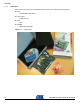
Overview 1.1.1 Deliverables Please unpack and inspect the AT91SAM7L-STK carefully and you will find the following items. Board – An AT91SAM7L-STK Board Power Supply – 2 AAA Batteries Cable – None CD ROM – SAM7L-STK CD ROM Figure 1-1. 1-2 6414A–ATARM–12-Sep-08 Unpacked Kit AT91SAM7L-STK Rev.
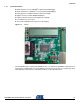
Overview 1.1.2 Starter Kit Features RS232 Interface to PC for SAM-BA® Programming and Debugging 20-pin ICE Interface to SAM-ICE™ for Programming and Debugging Battery Socket for 2 AAA Size Batteries 3.0V Power Supply ZigBee® Interface for Atmel AT86RF230 Adaptor Segment LCD (10 commons by 40 segments) for Display 5 Push Buttons for User’s Input User’s Grid and PIO Extension Interface for Prototyping Figure 1-2. Topview The AT91SAM7L-STK is supported by SAM-BA version 2.
Overview 1.1.3 Board Specification Table 1-1. AT91SAM7L-STK Specification 1-4 6414A–ATARM–12-Sep-08 Characteristic Specification Clock Speed Up to 36 MHz Ports RS232 Board Supply Voltage 1.8 to 3.6V DC Board Supply Current 18 mA typical (fully active, CPU at 36MHz) Temperature Operating Storage -10° to +50° C -40° to +85° C Relative Humidity 0 to 90% Dimensions 94 x 84 x 32 (L x W x H mm) RoHS Compliant AT91SAM7L-STK Rev.
Section 2 Setting Up the AT91SAM7L-STK Board 2.1 Electrostatic Warning The AT91SAM7L-STK evaluation board is shipped in protective anti-static packaging. The board must not be subjected to high electrostatic potentials. A grounding strap or similar protective device should be worn when handling the board. Avoid touching the component or any other metallic element. 2.2 Requirements In order to set up the AT91SAM7L-STK evaluation board, the following items are needed: 2.
Setting Up the AT91SAM7L-STK Board 2.4.0.2 DBGU Interface AT91SAM7L series Flash Microcontroller is able to boot from internal ROM or internal Flash memory through a general purpose NVM (GPNVM1) bit. When this bit is cleared, the MCU will boot from internal ROM to enable the SAM-BA connection through DBUG. Connect AT91SAM7L-STK DBGU port (J4) to PC COM port through an RS232 cable. Then you can run the SAM-BA from the PC to program the internal Flash of the MCU as well as the GPNVM1 bit.
Section 3 Development Tools 3.1 Overview This section offers a brief introduction to the hardware and software development tools required to test and develop custom applications on the AT91SAM7L-STK. Some development tools are needed as well for programming and debugging purposes. Refer to the user manuals of these tools for more information. 3.2 Typical Development Connection An RS232 serial cable is needed for DBGU SAM-BA communication.
Development Tools 3.4 SAM-ICE SAM-ICE is a JTAG emulator designed for all Atmel AT91SAM ARM7™/ARM9™ cores. DLL files to support SAM-ICE are available on the J-link ARM sub areas at www.segger.com. The J-Link software package is delivered as a ZIP file containing the setup program. After installation, SAM-ICE can be used in debugging. SAM-ICE Features: Any Atmel AT91SAM ARM7/ARM9 core supported, including Thumb mode. J-Link compatible mode. RDI compliant .
Development Tools 3.5 SAM-BA® SAM-BA (SAM Boot Assistant) is one of the tools provided in Atmel’s AT91 In-System Programming (ISP) solution. It provides an easy way for programming the AT91SAM family of microcontrollers using a graphical or command-line interface. It is also possible to create powerful scripts which can then be run via the command line, enabling the automation of many tasks. Those scripts can be hand written by the programmer or generated through the graphical user interface.
Development Tools 3.6 Sample Code and Technical Support Sample code can be downloaded and technical support is available on Atmel’s website www.atmel.com. Figure 3-3. 3-4 6414A–ATARM–12-Sep-08 View of the Atmel Website for AT91SAM Products AT91SAM7L-STK Rev.
Section 4 Board Description 4.
Board Description • Debug Unit (DBGU) • • • • • • • • • • • • • • • • • • 4-2 6414A–ATARM–12-Sep-08 – Two-wire UART and Support for Debug Communication Channel interrupt, Programmable ICE Access Prevention Periodic Interval Timer (PIT) – 20-bit Programmable Counter plus 12-bit Interval Counter Windowed Watchdog (WDT) – 12-bit Key-protected Programmable Counter – Provides Reset or Interrupt Signals to the System – Counter may be Stopped While the Processor is in Debug State or in Idle Mode Real-t
Board Description 4.2 AT91SAM7L64/128 Block Diagram Figure 4-1. AT91SAM7L64/128 Block Diagram TDI TDO TMS TCK ICE JTAG SCAN Charge Pump ARM7TDMI Processor JTAGSEL LCD Voltage Regulator System Controller 2 MHz RCOSC TST CAPP1 CAPM1 CAPP2 CAPM2 VDDINLCD VDD3V6 VDDLCD VDDIO2 IRQ0-IRQ1 PIO FIQ 1.
Board Description 4.3 Overview The AT91SAM7L-STK is designed to be a simple starter board for users to evaluate the performance and functionality of the AT91SAM7L-series microcontroller. Besides the basic system, the board integrates a 400-segments dot matrix LCD, segment LCD control being one of the main attributes of the AT91SAM7L, along with other low-power features. 4.4 Processor The AT91SAM7L-STK is equipped with an AT91SAM7L128 microcontroller in a 128 lead LQFP green package.
Board Description 4.5 Memory The AT91SAM7L128 embeds a total of 6 Kbytes high-speed SRAM, 128 Kbytes of high-speed internal Flash for programming and 12 Kbytes of ROM for SAM-BA support. 4.6 Clock Circuitry The clock generator of AT91SAM7L microcontroller is made up of one PLL, one fast RC oscillator, one slow oscillator and one 32,768 Hz crystal oscillator. To start up the system very quickly, the 2-MHz RC oscillator is automatically enabled after reset.
Board Description Figure 4-4. 4.7 Clock Circuit of the AT91SAM7L-STK Reset and Wake Up Circuitry There is one RESET button for external reset control of the AT91SAM7L128 and one WAKEUP button for waking the system up from off mode. The first time the board is powered, it will go directly into OFF mode. The WAKEUP button must be pushed to bring the chip out of OFF mode. After pushing the RESET button, the chip will go back into OFF mode. 4.7.
Board Description The battery power is supplied to VDDIO1 and VDDINLCD. The Main Voltage Regulator inside the chip will convert the supply from VDDIO1 to VDDOUT, to be supplied to VDDCORE for ARM7TDMI core supply. The internal Charge Pump inside the chip will convert the supply from VDDINLCD to a 3.6V VDD3V6, to be supplied to the VDDLCD pin for the Segment LCD controller. J8 is used for power-current measurement on the AT91SAM7L128 power supply. Figure 4-5.
Board Description Figure 4-6. LCD Regulator is Externally Supplied by Battery There is also a battery voltage monitor circuitry on the AT91SAM7L-STK board. The voltage is measured by AD3 of the AT91SAM7L128. This measurement bridge can be disconnected to save power consumption in OFF mode. This is under PC15 IO control as follows: PC15 = 0 enables the measurement bridge and half of the battery voltage is applied to AD3. PC15 = 1 or high impedance disables the measurement bridge. Figure 4-7.
Board Description 4.9 DBGU There is one serial debug port on the AT91SAM7L-STK for PC COM port connection for SAM-BA and serial communication through TXD and RXD signals. An auto-power-down RS232 transceiver, MAX3318E, is used on this board. When the board is powered on, SAM7L is in OFF mode and the FORCEOFF pin is pull-down by default so that the MAX3318E is in power down mode.
Board Description 4.11 Segment LCD The dot matrix LCD of the AT91SAM7L-STK is of type FSTN positive/reflective with 400 segments. It is controlled by the AT91SAM7L128 through 10 common signals and 40 segment signals. The contrast can be controlled by software, adjusting the LCD voltage regulator. Figure 4-10. Dot Matrix Segment LCD 4-10 6414A–ATARM–12-Sep-08 AT91SAM7L-STK Rev.
Board Description 4.12 User Buttons There are 5 user buttons on the AT91SAM7L-STK. The user buttons are connected to PIO lines and defined as 4-direction and ok buttons by default. Figure 4-11. User Buttons AT91SAM7L-STK Rev.
Board Description 4.13 ZigBee There is one ZigBee expansion interface for Atmel AT86RF230 ZigBee module. It is controlled via the SPI interface together with reset, interrupt and PIO control signals. Figure 4-12. ZigBee Interface Warning: The orientation of the connected circuit must be unambiguous. If the connected board is reversed, a short-circuit occurs between VCC and GND. 4-12 6414A–ATARM–12-Sep-08 AT91SAM7L-STK Rev.
Board Description 4.14 PIO Expansion The expansion connector of the AT91SAM7L-STK features the whole body of PIOC signals, ADC inputs, and ERASE pin. It enables users to expand functions such as SPI, TWI, PIO, ADC, USART, etc. With ERASE pin connected to VCC (short pin 39 and pin 40 by JS1), the internal Flash will be reinitialized upon system reset. Figure 4-13. PIOC Expansion Connector 4.
Section 5 Configuration The pages that follow contain detailed descriptions of PIO usage, jumpers, test points and solder drops on the AT91SAM7L-STK. 5.1 PIO Usage The AT91SAM7L128 microcontroller features three PIOs: PIOA, PIOB and PIOC. All Segment LCD controller signals are on PIOA and PIOB. PIOC and some of the PIOB IOs can be used fro peripheral signals such as SPI, TWI, PWM, USART, INT, etc. AT91SAM7L-STK Rev.
Configuration 5.1.1 PIOA Usage on the AT91SAM7L-STK Table 5-1.
Configuration 5.1.2 PIOB Usage on the AT91SAM7L-STK Table 5-2.
Configuration 5.1.3 PIOC Usage on the AT91SAM7L-STK Table 5-3.
Configuration 5.2 Jumpers Jumpers are used on the AT91SAM7L-STK for internal Flash Memory reinitialization and power current measurement. Table 5-4. Jumpers on AT91SAM7L-STK Designation Default Setting Feature J6 pins 39-40 Opened Erase Internal Flash (1) J8 Closed SAM7L VCC Jumper (2) J9 Closed Board VCC Jumper (3) Notes: 5.3 1. This jumper is used to erase the internal Flash and the associated NVM bits of the AT91SAM7L device. 2.
Configuration 5.4 Solder Drops Some solder drop selectors have been set on the AT91SAM7L-STK to enable alternate power supply schemes, such as selecting the internal charge pump to be used, or not, for the Segment LCD controller supply. Table 5-6.
Section 6 Schematics This section contains the following schematics: Top Level Synoptic Interface LCD, KBD Processor AT91SAM7L-STK Rev.
8 7 6 5 4 3 2 1 SHEET 2 Interfaces D D PC[0..29] PC[0..29] C C Interfaces SHEET 4 Processor AD[0..3] PA[0..25] PB[0..23] PC[0..29] AD[0..3] PA[0..25] PB[0..23] PC[0..29] ERASE Processor B B SHEET 3 LCD, KBD AD[0..3] PA[0..25] PB[0..23] PC[0..29] AD[0..3] PA[0..25] PB[0..23] PC[0..29] ERASE LCD, KBD A A B A REV AT91SAM7L-STK INIT EDIT MODIF. SCALE PP PP DES. 18-APR-08 17MAR08 DATE 1/1 This agreement is our property.
8 7 6 5 4 3 2 1 J2 Pad PC[0..
8 7 6 5 4 3 2 1 BP1 PC[0..29] PB[0..23] 3-1437565-0 PC1 UP PC0 OK PC2 RIGHT PC4 LEFT PC3 DOWN PA[0..
8 7 6 5 4 3 2 1 PC[0..
Section 7 Revision History Doc Rev Comments 6409A First issue. AT91SAM7L-STK Rev. B Starter Kit User Guide Change Request Ref.
Headquarters International Atmel Corporation 2325 Orchard Parkway San Jose, CA 95131 USA Tel: 1(408) 441-0311 Fax: 1(408) 487-2600 Atmel Asia Room 1219 Chinachem Golden Plaza 77 Mody Road Tsimshatsui East Kowloon Hong Kong Tel: (852) 2721-9778 Fax: (852) 2722-1369 Atmel Europe Le Krebs 8, Rue Jean-Pierre Timbaud BP 309 78054 Saint-Quentin-enYvelines Cedex France Tel: (33) 1-30-60-70-00 Fax: (33) 1-30-60-71-11 Atmel Japan 9F, Tonetsu Shinkawa Bldg.