
Datasheet


20
1919C–MICRO–3/05
AT89S52
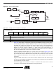
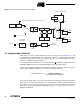
Figure 16-2. External Clock Drive Configuration
17. Program Memory Lock Bits
The AT89S52 has three lock bits that can be left unprogrammed (U) or can be programmed (P)
to obtain the additional features listed in Table 17-1.
When lock bit 1 is programmed, the logic level at the EA
pin is sampled and latched during reset.
If the device is powered up without a reset, the latch initializes to a random value and holds that
value until reset is activated. The latched value of EA
must agree with the current logic level at
that pin in order for the device to function properly.
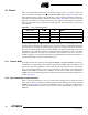
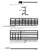
Table 16-1. Status of External Pins During Idle and Power-down Modes
Mode
Program
Memory ALE PSEN PORT0 PORT1 PORT2 PORT3
Idle Internal 1 1 Data Data Data Data
Idle External 1 1 Float Data Address Data
Power-down Internal 0 0 Data Data Data Data
Power-down External 0 0 Float Data Data Data
XTAL2
XTAL1
GND
NC
EXTERNAL
OSCILLATOR
SIGNAL
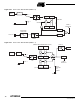
Table 17-1. Lock Bit Protection Modes
Program Lock Bits
LB1 LB2 LB3 Protection Type
1 U U U No program lock features
2PUU
MOVC instructions executed from external program memory
are disabled from fetching code bytes from internal memory, EA
is sampled and latched on reset, and further programming of
the Flash memory is disabled
3 P P U Same as mode 2, but verify is also disabled
4 P P P Same as mode 3, but external execution is also disabled