
User`s guide


Using the AT85DVK-07 Board
AT85DVK-07 Development Board User Guide 2-7
4391B–MP3–07/07
2.2 Power
Management
Unit
The Power Management unit allows three different power supply sources along with a
set of solder strap allowing configuration of “Very Low Voltage 1.8V application” or “Low
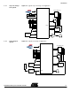
Voltage 3V application”. Figure 2-3 shows the power management unit implementation.
Jumpers J36, J37, J38, J39 must always be in place for proper operation and are imple-
mented for current measurement purpose only (see Section 2.14).
Figure 2-3. Power Management Unit Implementation
2.2.1 Battery Power
Supply
The AT85DVK-07 Board allows direct plug-in of a single AAA battery element or a AA
battery as an option.
Table 2-1. Battery Power Supply Range
2.2.2 External Power
Supply Connection
In order to operate without battery during firmware development process the AT85DVK-
07 Board provides an external power supply input through connector J20.
Notes: 1. Remove any plugged battery from the socket before applying the external voltage.
2. The external power supply input is not protected against polarization inversion.
Table 2-2. External Power Supply Connector Pinout (J20)
Table 2-3. External Power Supply Range
Figure 2-4. External Power Supply Cable
2.2.3 USB V
BUS
Power
Supply
The AT85C51SND3Bx provides direct connection of USB V
BUS
power supply. When
V
BUS
is present, the on-chip or on-board DC-DC is disabled to avoid battery power
consumption.
Table 2-4. USB V
BUS
Power Supply Range
J20
J36
LED
J38J39
J37
J22
J19
Power supply source Min. Max. Unit
Battery Power Supply 0.9 1.5 V
Pin Number Pin Name Pin Description
1 VBAT + 1.5V supply voltage
2 VSS 0V supply reference
Power supply source Min. Max. Unit
External Power Supply 0.9 3.0 V
+
-
+
-
Power supply source Min. Max. Unit
V
BUS
Power Supply 4.4 5.5 V