
User`s guide


Using the AT85DVK-07 Board
2-18 AT85DVK-07 Development Board User Guide
4391B–MP3–07/07
2.10 FM Receiver Unit
The FM unit consists in 2 extension connectors J1 & J2 (see Table 2-17 and Table 2-18)
allowing user to plug a daughter board featuring a FM receiver.
Note: Using P4.3:0 I/O port to control the FM receiver chip implies that the on-board DAC can
not be used in this configuration.
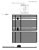
Table 2-17. FM Receiver Extension Connector (J1)
Table 2-18. FM Receiver Extension Connector (J2)
2.11 Display Unit
The Display unit consists in a 128x64 monochrome pixels LCD. It is possible to plug a
daughter board equipped with an other LCD (color, higher resolution…) using J11 con-
nector (see Section 2.4.2).
Note: On-board LCD must be disconnected before plugging any daughter boards.
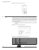
2.12 Keypad Unit
The Keypad unit consists in a 3 x 4 key matrix including a 4-direction mini joystick and
power-on key along with 2 extension connectors. J10 & J30 allow user to plug a daugh-
ter board featuring particular keys like 2-direction mini joystick, rolling wheel…
Note: To ease software implementation with generic software keypad driver, user’s keypad
arrangement must fit with an available matrix configuration (for further information, refer
to the firmware user’s manual).
Figure 2-18. Keypad Unit Implementation
Pin Number Pin Name Pin Description
1 VDD IOVDD power supply 1.8V or 3V depending on the power configuration
2 LINL Left channel analog input
3 LINC Common reference analog input
4 LINR Right channel analog input
5 AVSS 0V analog supply reference
6 AVSS 0V analog supply reference
Pin Number Pin Name Pin Description
1 VDD IOVDD power supply 1.8V or 3V depending on the power configuration
2 P4.0/OCLK FM receiver control bit 0
3 P4.1/DCLK FM receiver control bit 1
4 P4.2/DDAT FM receiver control bit 2
5 P4.3/DSEL FM receiver control bit 3
6 VSS 0V digital supply reference
J10
J30
F1
F2