
User`s guide


Using the AT85DVK-07 Board
AT85DVK-07 Development Board User Guide 2-15
4391B–MP3–07/07
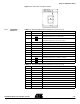
Figure 2-14. MMC/SD Unit Implementation
2.7.1 MMC I/O Extension Two extension connectors J31 and J32 (see Table 2-13 and Table 2-14) are imple-
mented to get an access to the P2 alternate I/Os in case MMC is not used, or to plug an
other socket (e.g. Mini-SD) through a daughter board.
Table 2-13. MMC/SD I/O Extension Connector (J31)
Table 2-14. MMC/SD I/O Extension Connector (J32)
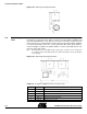
2.8 Audio Input Unit
The Audio Input unit consists in the electret microphone unit and a 3.5mm stereo input
jack J3.
J32
J31
J28
P2
P2
MMC/SD
Pin Number Pin Name Pin Description
1 P2.0/SDINS SD/MMC Card Insertion Signal
2 P2.1/SDLCK SD Card Write Lock Signal
3 P2.2/SDCMD SD/MMC Command Line
4 P2.3/SDCLK SD/MMC Clock
5 P2.4/SDDAT0 SD/MMC Data Line 0
Pin Number Pin Name Pin Description
1 P2.5/SDDAT1 SD/MMC Data Line 1
2 P2.6/SDDAT2 SD/MMC Data Line 2
3 P2.7/SDDAT3 SD/MMC Data Line 3
4 VDD IOVDD power supply 1.8V or 3V depending on the power configuration
5 VSS 0V digital supply reference