
User`s guide


Using the AT85DVK-07 Board
AT85DVK-07 Development Board User Guide 2-13
4391B–MP3–07/07
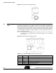
Figure 2-11. Nand Flash Unit Implementation
2.6.1 Nand Flash
Extension
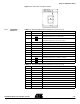
Table 2-11. Nand Flash Daughter Board Extension Connector (J13)
Table 2-12. Nand Flash Daughter Board Extension Connector (J14)
J14
J13
NF
Footprint
Pin Number Pin Name Pin Description
1 NFWP Write Protect Signal
2
NFCE3
SMCE
Nand Flash 3 Chip Enable
SmartMediaCard/xD-Picture Card Chip Enable
3
NFCE2
SMINS
Nand Flash 2 Chip Enable
SmartMediaCard/xD-Picture Card Insertion Signal
4 NFWP Write Protect Signal
5 VDD IOVDD power supply 1.8V or 3V depending on the power configuration
6 NFCLE Command Latch Enable Signal
7 NFALE Address Latch Enable Signal
8 NC Not Used
9 NFCE0 Nand Flash 0 Chip Enable
10 NC Not Used
11
NFCE1
SMLCK
Nand Flash 1 Chip Enable
SmartMediaCard/xD-Picture Card Write Lock Signal
12 NFRE Read Enable Signal
13 NFWE Write Enable Signal
Pin Number Pin Name Pin Description
1 NFWP Write Protect Signal
2 NC Not Used
3 NC Not Used
4 NFWP Write Protect Signal
5 NFD7 Data Bit 7
6 NFD6 Data Bit 6
7 NFD5 Data Bit 5
8 NFD4 Data Bit 4
9 NFD3 Data Bit 3
10 NFD2 Data Bit 2