
User Manual


Atmel AT03911: REB233CBB Module – User Manual [APPLICATION NOTE]
42156BWIRELESS02/2014
4
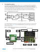
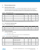
5. Functional description
The block diagram of the REB233CBB Module is shown in Figure 5-1. The Radio PCB and Microcontroller PCB are
connected via a mounting header. The Radio PCB is not functional without connecting it correctly to the Microcontroller
PCB. The Radio PCB is equipped with two approved antennas; see B.3 and [2], to enable antenna diversity (AD)
operation.The Microcontroller PCB controls the Radio PCB, provides the power supply as well as the user interface. The
user interface consists of three LEDs and two pushbuttons for manual user control of the module. Additional
microcontroller (MCU) GPIOs, like USART, UART and JTAG, are available to control the module with a host-PC.
Figure 5-1. REB233CBB Module block diagram
AT86RF233
SMA1
SMA2
ANT1
ANT2
GPIORF1
SPI
Switch
RF2
RF
ATxmega256A3
Battery
Interface
LEDs
Buttons
Radio PCB Microcontroller PCB User Interface
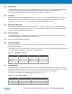
The two REB233CBB Module components, the Radio PCB, equipped with two swivel antennas, and Microcontroller
PCB, are shown in detail in Figure 5-2. Here, the REB233CBB Module is dismounted for better explanation of all
important hardware features.
Figure 5-2. REB233 Module features (dismounted view for better description)
Radio PCB
Microcontroller PCB
Battery holder
JTAG
Power switch
UART
LEDs
Buttons
GPIOs
ANT1
SMA1
Mounting header
SMA2
ANT2
OFF
ON