
User's Manual

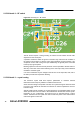


Table Of Contents
- 1 Introduction
- 2 Disclaimer
- 3 Overview
- 4 Functional description
- 5 PCB layout description
- 6 Mechanical description
- 7 Electrical characteristics
- 8 Abbreviations
- References
- EVALUATION BOARD/KIT IMPORTANT NOTICE
- 9 Table of contents

14
Atmel AVR2092
8427A-AVR-10/11
Figure 5-5. Board layout – transceiver GND.
30
31
32
27
6 3
12
7
16
18 21
The soldering technology used allows the placement of small vias (0.15mm drill)
within the ground paddle underneath the chip. During reflow soldering, the vias get
filled with solder, having a positive effect on the connection cross section. The small
drill size keeps solder losses within an acceptable limit. During the soldering process
vias should be open on the bottom side to allow enclosed air to expand.
5.5 PCB detail 5 – digital GND routing and shielding
With the Atmel AT86RF232, consider pins 7, 12, 16, 18, and 21 as digital ground
pins.
Digital ground pins are not directly connected to the paddle. Digital ground pins may
carry digital noise from I/O pad cells or other digital processing units within the chip.
In case of a direct paddle connection, impedances of the paddle ground vias could
cause a small voltage drop for this noise and may result in an increased noise level
transferred to the analog domain.
There is a number of pro’s and con’s when it comes to the shielding topic. The major
con’s are:
• Cost of the shield
• Manufacturing effort
• Inaccessibility for test and repair
The number of pro’s might be longer but the cost argument is often very strong.
However, the reasons to add the shield for this reference design are:
• Shield is required for a certification in Japan
• Shield is recommended for FCC certification in North America
• Increased performance