
User's Manual

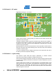


Table Of Contents
- 1 Introduction
- 2 Disclaimer
- 3 Overview
- 4 Functional description
- 5 PCB layout description
- 6 Mechanical description
- 7 Electrical characteristics
- 8 Abbreviations
- References
- EVALUATION BOARD/KIT IMPORTANT NOTICE
- 9 Table of contents

Atmel AVR2092
13
8427A-AVR-10/11
Figure 5-4. Board layout – XTAL section.
The reference crystal and load capacitors C36/37 form the resonator circuit. These
capacitors are to be placed close to the crystal. The ground connection in between
the capacitors should be a solid copper area right underneath the crystal, including
the housing contacts.
5.4 PCB detail 4 – transceiver analog GND routing
With the Atmel AT86RF232, consider pins 3, 6, 27, 30, 31, and 32 as analog ground
pins.
Analog ground pins are to be routed to the paddle underneath the IC. The trace width
has to be similar to the pad width when connecting the pads, and increase, if
possible, in some distance from the pad.
Each ground pin should be connected to the bottom plane with at least one via. Move
the vias as close to the IC as possible. It is always desired to integrate the single-pin
ground connections into polygon structures after a short distance. Top, bottom, and,
on multilayer boards, the inner ground planes, should be tied together with a grid of
vias. When ground loops are smaller than one tenth of the wavelength, it is safe to
consider this as a solid piece of metal.