
User's Manual

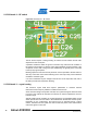


Table Of Contents
- 1 Introduction
- 2 Disclaimer
- 3 Overview
- 4 Functional description
- 5 PCB layout description
- 6 Mechanical description
- 7 Electrical characteristics
- 8 Abbreviations
- References
- EVALUATION BOARD/KIT IMPORTANT NOTICE
- 9 Table of contents

12
Atmel AVR2092
8427A-AVR-10/11
5.2 PCB detail 2 – RF switch
Figure 5-3. Board layout – RF switch.
RF RF
RF
The RF switch requires a solid grounding to achieve the full isolation and RF filter
capacitors for the control pins.
A parasitic inductance within the ground connection may reduce the RF isolation of
the switch in the off state. To achieve a hard, low-impedance ground connection, vias
are placed on each side of the ground pad. Additionally, the ground pad is connected
to the top layer ground plane.
Blocking capacitors C24 and C25 are placed as close as possible to the RF switch to
short any control line noise. Noise interfering on the control pins may cause undesired
modulation of the RF signal.
C11 and C12 will block any DC voltage on the RF line. On the input side, C28, next to
the balun provides the required DC blocking.
5.3 PCB detail 3 – crystal routing
The reference crystal PCB area requires optimization to minimize external
interference and to keep any radiation of 16MHz harmonics low.
Since the board design incorporates a shield, the crystal housing has been tied hard
to ground. This method will minimize the influence of external impairments such as
burst and surge.
Against board internal crosstalk, the crystal signal lines are embedded within ground
areas. Special care has to be taken in the area between the IRQ line and the crystal.
Depending on the configuration, the interrupt may be activated during a frame
receive. Crosstalk into the crystal lines will increase the phase noise and therefore
reduce the signal to noise ratio.