
User's Manual
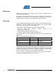
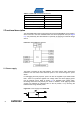
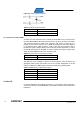
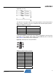
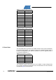
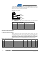
Table Of Contents

AVR2042
9
8334A-AVR-11/10
Table 5-10. AT25DF021 ordering information.
Ordering Code Flash Maximum freq. Power supply Package Temperature
AT25DF021-SSHF-B 256KB + 8KB 50MHz 2.3V – 3.6V 8S1 SOP-8 -40°C – 85°C
5.6 UART
The serial asynchronous interface, USARTD0, of the Atmel ATxmega256A3 is
connected to header USARTD0. Additionally, the MCU reset line is connected to pin
5 of the header. This can be used to work with a serial boot loader. No level
conversion is done; therefore, an external RS232/TTL conversion circuit is required.
The header pin-out mates with the available RS232/TTL converter (art. no. de28560).
Table 5-11. Connection of USARTD0.
ATxmega256A3 Header USARTD0 Description
PD2 (28) RxD (4) Asynchronous serial in
PD3 (29) TxD (1) Asynchronous serial out
RESET (57) RESET (5) MCU reset
6 Programming
On the ATxmega256A3, both programming and debugging can be done through two
physical interfaces.
The primary interface is the program and debug interface (PDI). This is a two-pin
interface using the reset pin for the clock input (PDI_CLK) and the dedicated test pin
for data input and output (PDI_DATA).
Programming and debugging can also be done through the four-pin JTAG interface.
The JTAG interface is IEEE 1149.1 standard compliant and supports boundary scan.
Any external programmer or on-chip debugger/emulator can be directly connected to
these interfaces, and no external components are required.
The Atmel REB-CBB provides a 10-pin header to connect the Atmel JTAGICE mkII
probe. This connection can be used for both protocols, JTAG and PDI.
Figure 6-1. Connection between JTAGICE mkII and REB-CBB.
DBGSEL