
User's Manual
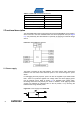
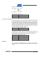
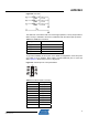
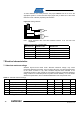
Table Of Contents

10
AVR2042
8334A-AVR-11/10
To select between one of the protocols, the jumper DBGSEL has to be set to the
appropriate position. It routes test data input (signal TDI) to either TDI of the JTAG
interface or PDI of Atmel’s proprietary PDI interface.
Figure 6-2. Debug interface.
Note: Atmel JTAGICE mkII units with hardware revision 0 do not have PDI
capabilities.
Table 6-1. Connection of header DBG.
DBG Connector DBGSEL=JTAG DBGSEL=PDI
TMS (5) PB4 (10) PB4 (10) unused
TDI (9) PB5 (11) PDI (56)
TCK (1) PB6 (12) PB6 (12) unused
TDO (3) PB7 (13) PB7 (13) unused
nSRST (6) RESET (57) RESET (57)
7 Electrical characteristics
7.1 Absolute maximum ratings
Stresses beyond those listed under “Absolute maximum ratings” may cause
permanent damage to the board. This is a stress rating only, and functional operation
of the device at these or any other conditions beyond those indicated in the
operational sections of this manual are not implied. Exposure to absolute maximum
rating conditions for extended periods may affect device reliability. For more details
about these parameters, refer to individual datasheets of the components used.
Table 7-1. Absolute maximum ratings.
No. Parameter Condition Minimum Typical Maximum Units
7.1.1 Storage temperature range -40 +85 °C
7.1.2 Humidity Non-condensing 90 %
7.1.3 Supply voltage -0.3 +3.6 V
7.1.4 EXT I/O pin voltage -0.3 Vcc + 0.3 V
7.1.5 Supply current from batteries Sum over all power pins -0.5 A
7.1.6 Battery charge current
(1)
0 mA
Note: 1. Keep power switch off or remove battery from REB-CBB when external power is supplied.
RST
PDI
TDI
TMS
TDO
TCK
DBGSEL
1
3
5
6
9
DBG
PDI
JTAG