
User's Manual
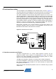
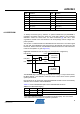
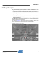
Table Of Contents

AVR2043
7
8345A-AVR-11/10
Depending on the actual supply voltage, the diode D1 can consume several
milliamperes. This has to be considered when the current consumption of the whole
system is measured. In such a case, D1 should be removed from the board.
To achieve the best RF performance, the analog (EVDD, AGND) and digital (DEVDD,
DGND) supply are separated from each other by a CLC PI-element. Digital and
analog ground planes are connected together on the bottom layer, underneath the
radio transceiver IC. Further details are described in Section 5, pag
e 9.
A jumper, JP1, is placed in the supply voltage trace to offer an easy way for current
sensing to occur.
NOTE All components connected to nets DEVDD/EVDD contribute to the total current
consumption.
While in radio transceiver SLEEP state, most of the supply current is drawn by the
1M pull-up resistor, R9, connected to the ID EEPROM and the EEPROM standby
current.
Figure 4-4. Power supply routing.
4.4 Radio transceiver reference clock
The integrated radio transceiver is clocked by a 16MHz reference crystal. The
2.4GHz modulated signal is derived from this clock. Operating the node according to
IEEE 802.15.4 [4], the ref
erence frequency must not exceed a deviation of ±40ppm.
The absolute frequency is mainly determined by the external load capacitance of the
crystal, which depends on the crystal type and is given in its datasheet.
The radio transceiver reference crystal, Q1, shall be isolated from fast switching
digital signals and surrounded by a grounded guard trace to minimize disturbances of
the oscillation. Detailed layout considerations can be found in Section 5.3, page 11.
The
REB uses a Siward CX4025 crystal with load capacitors of 10pF and 12pF. The
imbalance between the load capacitors was chosen to be as close as possible to the
desired resonance frequency with standard components. To compensate for
fabrication and environment variations, the frequency can be further tuned using the
radio transceiver register XOSC_CTRL (0x12) (refer to [1], Section References, page
30). The RE
B production test guarantees a tolerance of within +20ppm and -5ppm.
The correction value, to be applied to TRX register XOSC_CTRL (0x12), is stored in
the onboard EEPROM (see Section 4.2, page 5).
The reference frequ
ency is also available at pin CLKM of the radio transceiver and,
depending on the related register setting, it is divided by an internal prescaler. CLKM
clock frequencies of 16MHz, 8MHz, 4MHz, 2MHz, 1MHz, 250kHz, or 62.5kHz are
programmable (refer to [1]). The
CLKM signal is filtered by a low-pass filter to reduce
harmonic emissions within the 2.4GHz ISM band. The filter is designed to provide a
stable 1MHz clock signal with correct logic level to a microcontroller pin with
sufficiently suppressed harmonics. CLKM frequencies above 1MHz require a