
User's Manual
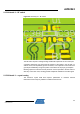
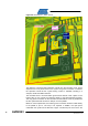
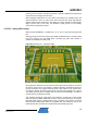
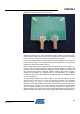
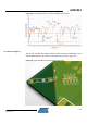
Table Of Contents

14
AVR2043
8345A-AVR-11/10
5.5 PCB – digital GND routing
With the Atmel AT86RF231, consider pins 7, 12, 16, 18, and 21 as digital ground
pins.
Digital ground pins are not directly connected to the paddle. Digital ground pins may
carry digital noise from I/O pad cells or other digital processing units within the chip.
In case of a direct paddle connection, impedances of the paddle ground vias could
cause a small voltage drop for this noise and may result in an increased noise level
transferred to the analog domain.
5.6 PCB – GND plane
Besides the function to provide supply ground to the individual parts, the ground
plane has to be considered as a counterpart for the antenna. Such an antenna base
plate is considered a continuous metal plane.
For that reason, any unused surface should be filled with a copper plane and
connected to the other ground side using sufficient through holes. Larger copper
areas should also be connected to the other side layer with a grid of vias. This way,
for an external EM field, the board will behave like a coherent piece of metal.
When a trace is cutting the plane on one side, the design should contain vias along
this trace to bridge the interrupted ground on the other side. Place vias especially
close to corners and necks to connect lose polygon ends.
5.7 Ceramic antenna
5.7.1 Antenna design study
Part of the diversity board development was the evaluation of the antenna setup. A
dedicated board was designed to determine the key design parameters for a diversity
antenna configuration.
Because the antenna has to operate in an environment different from that of the
manufacturer’s evaluation board, the correct frequency tuning has to be verified. The
antenna distance, required for optimum diversity operation, provides enough board
space to use a low-cost tuning method based on a transmission line and capacitors.
The actual tuning procedure is explained in Section 5.7.3, page 18.