
User's Manual
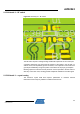
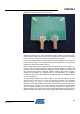
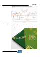
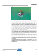
Table Of Contents

AVR2043
11
8345A-AVR-11/10
5.2 PCB detail 2 – RF switch
Figure 5-3. Board layout – RF switch.
The RF switch requires a solid grounding and RF filter capacitors for the control pins.
A parasitic inductance may reduce the RF isolation of the switch in the off state. To
achieve a hard, low-impedance ground connection, a via is placed on each side of the
ground pad. Additionally, the ground pad is connected to the top layer ground plane.
Blocking capacitors C38 and C39 are placed as close as possible to the RF switch to
short any control line noise, avoiding parasitic amplitude modulation of the RF signal.
5.3 PCB detail 3 – crystal routing
The reference crystal PCB area requires optimization to minimize external
interference and to keep any radiation of 16MHz harmonics low.