
User's Manual Part 1

13,56 MHz Multitag Reader Module, Version 0.9v
ACG Identification Technologies AT Page 1
Table of Content
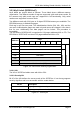
1 Scope ..................................................................................................3
2 Definitions and abbreviations ...........................................................4
2.1 Definitions:......................................................................................................... 4
2.1.1 Anticollision loop......................................................................................... 4
2.1.2 Hex notation................................................................................................ 4
2.1.3 ASCII notation............................................................................................. 4
2.2 Abbreviations..................................................................................................... 4
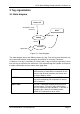
3 Tag organization.................................................................................5
3.1 State diagram.................................................................................................... 5
3.2 Supported labels ............................................................................................... 6
3.3 ISO 15693......................................................................................................... 7
3.3.1 Coding of UID ............................................................................................. 7
3.3.2 Memory organization .................................................................................. 7
3.3.3 My-D Label (SRF55VxxP)........................................................................... 8
3.3.4 EM 4135 ..................................................................................................... 9
3.4 Icode®............................................................................................................... 9
3.4.1 Memory organization .................................................................................. 9
3.4.2 Serial number ............................................................................................. 9
3.4.3 Write access condition.............................................................................. 10
3.4.4 Special function (EAS), AFI ...................................................................... 10
3.4.5 User data .................................................................................................. 10
3.5 TAGIT®........................................................................................................... 10
3.6 SR176 ............................................................................................................. 11
3.6.1 Memory organization ................................................................................ 11
3.6.2 Serial number UID .................................................................................... 11
3.6.3 Lock byte .................................................................................................. 11
3.6.4 Chip ID...................................................................................................... 11
3.7 ISO 14443....................................................................................................... 12
3.8 Mifare® Ultralight............................................................................................. 12
3.8.1 Memory organization ................................................................................ 12
3.8.2 Serial number ........................................................................................... 12
3.8.3 Lock bytes................................................................................................. 13
3.8.4 OTP bytes................................................................................................. 13
3.8.5 User data .................................................................................................. 13
4 Hardware...........................................................................................14
4.1 Pin out of OEM Module ................................................................................... 14
4.1.1 Pin out of J1.............................................................................................. 14
4.1.2 Pin out of J2.............................................................................................. 15
4.1.3 Electrical characteristics of PINs............................................................... 15
5 Software............................................................................................16
5.1 ASCII Protocol................................................................................................. 16
5.2 Binary Protocol................................................................................................ 16
5.2.1 STX........................................................................................................... 16
5.2.2 Station ID.................................................................................................. 16
5.2.3 Length....................................................................................................... 16
5.2.4 Data.......................................................................................................... 16
5.2.5 Block Check Character (BCC) .................................................................. 16