
Specifications


www.ti.com
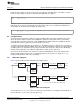
Standard Initialization Sequence for Hercules Microcontrollers
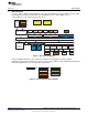
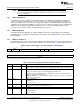
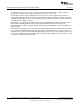
The clock source disable register (CSDISSET) is shown in Figure 7.
Figure 7. Clock Source Disable Set Register (CSDISSET) Address = 0xFFFFFF34
31 16
Reserved
R-0
15 8 7 6 5 4 3 2 1 0
SET SET SET SET SET SET SET SET
CLK CLK CLK CLK CLK CLK CLK CLK
Reserved
SR7 SR6 SR5 SR4 SR3 SR2 SR1 SR0
OFF OFF OFF OFF OFF OFF OFF OFF
R-0 R/WP-1 R/WP-1 R/WP-0 R/WP-0 R/WP-1 R/WP-1 R/WP-1 R/WP-0
LEGEND: R = Read in all modes; WP = Write in priviledged mode only; -n = value after reset; D = Device-specific reset value
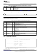
The clock source disable clear register (CSDISCLR) is shown in Figure 8.
Figure 8. Clock Source Disable Clear Register (CSDISCLR) Address = 0xFFFFFF38
31 16
Reserved
R-0
15 8 7 6 5 4 3 2 1 0
CLR CLR CLR CLR CLR CLR CLR CLR
CLK CLK CLK CLK CLK CLK CLK CLK
Reserved
SR7 SR6 SR5 SR4 SR3 SR2 SR1 SR0
OFF OFF OFF OFF OFF OFF OFF OFF
R-0 R/WP-1 R/WP-1 R/WP-D R/WP-0 R/WP-1 R/WP-1 R/WP-1 R/WP-0
LEGEND: R = Read in all modes; WP = Write in priviledged mode only; -n = value after reset; D = Device-specific reset value
• The system module also contains two additional registers that can be used to enable or disable clock
sources. These registers are provided so that the application can avoid using read-modify-write
operations for enabling or disabling clock sources.
• Setting any bit in the CSDISSET register commands the corresponding clock source to be disabled.
• Setting any bit in the CSDISCLR register enables the corresponding clock source.
2.3.3 Example Clock Source Configuration
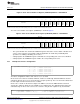
systemREG1->CSDISCLR = 0x00000000U
| 0x00000001U // Enable clock source 0
| 0x00000002U // Enable clock source 1
| 0x00000010U // Enable clock source 4
| 0x00000020U // Enable clock source 5
| 0x00000040U; // Enable clock source 6
The above configuration enables clock sources 0, 1, 4, 5, and 6.
Of the clock sources that are enabled, number 0, 4 and 5 are enabled by default and will have become
valid by the time the processor is released from reset upon a power-up. These are the main oscillator and
the two outputs from the internal reference oscillator.
Clock source 1 and 6 are the two PLL outputs. The FMPLL as well as the FMPLL#2 have a defined
start-up time, and their outputs are not available for use until this time. The application must wait for the
valid status flags for these clock sources to be set before using the PLL outputs for any clock domain.
while (!((systemREG1->CSVSTAT & 2) // Wait for FMPLL to become valid
& (systemREG1-> CSVSTAT & 0x40))); // Wait for FMPLL#2 to become valid
9
SPNA106– September 2011 Initialization of Hercules™ ARM
®
Cortex™-R4F Microcontrollers
Submit Documentation Feedback
Copyright © 2011, Texas Instruments Incorporated