
Specifications
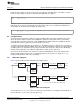


Standard Initialization Sequence for Hercules Microcontrollers
www.ti.com
2.3 Enable Clock Sources
2.3.1 Available Clock Sources on Hercules Microcontrollers
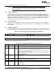
The Hercules microcontrollers support seven different clock sources, as listed in Table 3.
Table 3. Clock Sources on Hercules Microcontrollers
Clock
Source
Number Clock Source Name Description
This is the primary oscillator, typically driven by an external resonator or crystal. This
0 OSCIN is the only available input to the FMPLL and the FMPLL2 macros. The OSCIN
frequency must be between 5 MHz and 20 MHz.
This is the output of the FMPLL, which is generated using the OSCIN as the input
clock. The FMPLL output clock frequency must not exceed the maximum device
1 FMPLL#1 output
frequency specified in the specific part's datasheet. The FMPLL features a modulation
mode where a modulation frequency is superimposed on the FMPLL output signal.
No clock signal is connected to source # 2. This clock source must not be enabled or
2 Not implemented
chosen for any clock domain.
External clock input # 1. This clock source must only be enabled if there is an actual
3 EXTCLKIN1 external clock source connected to the identified device terminal for EXTCLKIN1. For
more information, see the specific part's datasheet.
This is the low-frequency output of the internal reference oscillator. The LF LPO is
4 LF LPO
typically an 80 KHz signal, and is generally used for low-power mode use cases.
This is the high-frequency output of the internal reference oscillator. The HF LPO is
5 HF LPO typically a 10 MHz signal, and is used as a reference clock for monitoring the main
oscillator.
This is the output of the secondary FMPLL, which is generated using the OSCIN as
6 FMPLL#2 output the input clock. The FMPLL output clock frequency must not exceed the maximum
device frequency specified in the specific part's datasheet.
External clock input # 2. This clock source must only be enabled if there is an actual
7 EXTCLKIN2 external clock source connected to the identified device terminal for EXTCLKIN2. For
more information, see the specific part's datasheet.
2.3.2 Control Registers for Enabling and Disabling Clock Sources
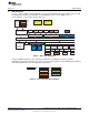
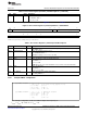
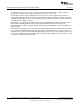
Figure 6 shows the default states of the clock sources supported on the Hercules microcontrollers:
• Clock sources 0, 4 and 5 are enabled, while clock sources 1, 3, 6 and 7 are disabled upon any system
reset.
• Clock source 2 is not implemented and must not be enabled in the application.
The clock source disable register (CSDIS) is shown in Figure 6.
Figure 6. Clock Source Disable Register (CSDIS) Address = 0xFFFFFF30
31 16
Reserved
R-0
15 8 7 6 5 4 3 2 1 0
CLK CLK CLK CLK CLK CLK CLK CLK
Reserved SR7 SR6 SR5 SR4 SR3 SR2 SR1 SR0
OFF OFF OFF OFF OFF OFF OFF OFF
R-0 R/WP-1 R/WP-1 R/WP-D R/WP-0 R/WP-1 R/WP-1 R/WP-1 R/WP-0
LEGEND: R = Read in all modes; WP = Write in priviledged mode only; -n = value after reset; D = Device-specific reset value
• Each bit of the CSDIS controls the clock source of the same number: bit 0 controls clock source 0, bit
1 controls clock source 1, and so on.
• Setting any bit commands, the corresponding clock source to be disabled.
– The clock source can only be disabled once there is no clock domain or secondary clock source
(FMPLL, FMPLL#2) using the clock source to be disabled.
8
Initialization of Hercules™ ARM
®
Cortex™-R4F Microcontrollers SPNA106– September 2011
Submit Documentation Feedback
Copyright © 2011, Texas Instruments Incorporated