
Specifications


www.ti.com
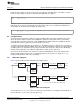
Standard Initialization Sequence for Hercules Microcontrollers
Table 1. PLL Control Register (PLLCTL1) Field Descriptions (continued)
Bit Field Value Description
15-0 PLLMUL Defines the NF multiplier
NF = (PLLMUL / 256) + 1
f
VCOCLK
= f
INTCLK
* NF
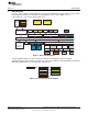
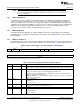
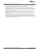
The PLL control register 2 (PLLCTL2) is shown in Figure 5 and described in Table 2.
Figure 5. PLL Control Register 2 (PLLCTL2) Address = 0xFFFFFF74
31 30 22 21 20 16
FM
SPREADINGRATE[8:0] RSVD MULMOD[8:4]
ENA
R/WP-0 R/WP-0x1FF RW-0 R/WP-0x000
15 12 11 9 8 0
MULMOD[3:0] ODPLL SPR_AMOUNT[8:0]
R/WP-0x000 R/WP-111b R/WP-0x000
LEGEND: R = Read; W = Write; P = Priviledge mode only; -n = value after reset
Table 2. PLL Control Register 2 (PLLCTL2) Field Descriptions
Bit Field Value Description
31 FM ENA Setting the FM ENA bit enables the modulation frequency to be superimposed on the output
of the FMPLL macro.
30-22 SPREADINGRATE Defines the modulation frequency used
NS = SPREADINGRATE + 1
Modulation frequency, f
mod
= fs = f
INTCLK
/ (2 * NS)
21 Reserved 0 Reserved
20-12 BWADJ Defines the FMPLL modulation bandwidth adjustment
NB = BWADJ + 1
f
BW
= f
nom_BW
/ NB
NOTE: NB must be set to 7 when modulation is not used. This is also the default value.
11-9 ODPLL Defines the OD-divider
OD = ODPLL + 1
f
post-ODCLK
= f
VCOCLK
/ OD
8-0 SPR_AMOUNT Defines the frequency modulation depth divider.
NV = SPR_AMOUNT + 1
2.2.4.1 Example FMPLL Configuration
systemREG1->PLLCTL1 = 0x00000000U
| 0x20000000U // No reset on slip, bypass on slip
| (0U << 24U) // R = 1
| (5U << 16U) // NR = 6
| (119U << 8U); // NF = 120
systemREG1->PLLCTL2 = 0x00000000U // Modulation disabled
| (255U << 22U) // NS = 256
| (7U << 12U) // NB = 8
| (1U << 9U) // OD = 2
| 61U; // NV = 62
This example configuration results in a FMPLL output clock frequency of:
f
PLLCLK
= (f
OSCIN
/ 6) * 120 / 2 / 1 = f
OSCIN
* 10
7
SPNA106– September 2011 Initialization of Hercules™ ARM
®
Cortex™-R4F Microcontrollers
Submit Documentation Feedback
Copyright © 2011, Texas Instruments Incorporated