
Specifications


Standard Initialization Sequence for Hercules Microcontrollers
www.ti.com
2.18 Run Self-Test on the Flash Module SECDED Logic
The Flash module reads the “reset configuration vector” from address 0xF0080140 in the TI OTP region of
Flash bank 0. This is a 64-bit value which is used to configure the device power domains, etc. The Flash
module has built-in SECDED logic to correct any single-bit error in this vector or detect and flag and
double-bit error in this vector. If a double-bit error is detected during this read from the OTP, an ESM
(Error Signaling Module) group3 error condition is flagged and the nERROR signal is asserted low. If a
single-bit error is detected during the read from the OTP, this error is corrected by the SECDED logic – no
flag is set and no error signal is sent to the ESM.
The following sequence can be used to verify that the reset configuration vector was read in correctly by
the Flash module:
• The error checking logic in the Flash module is disabled by default and must be enabled. This can be
done by writing 0xA to the EDACEN[3 – 0] field of the FEDACCTRL1 control register at address
0xFFF87008.
• Read the 64-bit reset configuration vector from address 0xF0080140.
• Check for any single-bit or double-bit error flags.
There is also a procedure for running an elaborate self-test on the SECDED logic inside the Flash module.
This procedure is described in the Flash Module chapter of the specific part's technical reference manual.
2.19 On-Chip SRAM Auto-Initialization
The system module on the Hercules microcontroller allows all on-chip SRAMs to be initialized in hardware.
This is especially essential since all the on-chip memories support some form of error detection. The CPU
data RAM supports ECC while the peripheral memories support parity error detection. The
auto-initialization mechanism also initializes the ECC or parity memories, as required. The following
registers are used in this process.
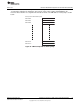
The memory hardware initialization global control register (MINITGCR) is shown in Figure 22 and
described in Table 13.
Figure 22. Memory Hardware Initialization Global Control Register (MINITGCR) Address =
0xFFFFFF5C
31 16
Reserved
R-0
15 4 3 0
Reserved MINITGENA[3:0]
R-0 R/WP-0101
LEGEND: R = Read in all modes; WP = Write in priviledged mode; -n = value after reset
Table 13. Memory Hardware Initialization Global Control Register (MINITGCR) Field Descriptions
Bit Field Value Description
31-4 Reserved 0 Reserved
3-0 MINITGENA Must be configured to 1010b to enable the hardware memory initialization mechanism
The memory self-test / initialization control register (MSIENA) is shown in Figure 23 and described in
Table 14.
24
Initialization of Hercules™ ARM
®
Cortex™-R4F Microcontrollers SPNA106– September 2011
Submit Documentation Feedback
Copyright © 2011, Texas Instruments Incorporated