
Specifications


Standard Initialization Sequence for Hercules Microcontrollers
www.ti.com
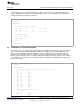
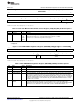
Table 11. GCLK, HCLK , VCLKx Source Register (GHVSRC) Field Descriptions (continued)
Bit Field Value Description
23-20 Reserved 0 Reserved
19-16 HVLPM Defines the clock source used for the HCLK and VCLKx domains when the CPU clock domain
GCLK is disabled.
15-1 Reserved 0 Reserved
0 GHVSRC Defines the clock source to be currently used for the GCLK, HCLK and VCLKx domains. As shown
by the reset value of the GHVSRC field, the clock source # 0, that is, the main oscillator, is used as
the default clock source for the GCLK, HCLK and VCLKx domains.
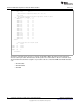
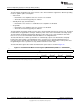
The asynchronous clock source register (VCLKASRC) is shown in Figure 17 and described in Table 12.
Figure 17. Asynchronous Clock Source Register (VCLKASRC) Address = 0xFFFFFF4C
31 16
Reserved
R-0
15 12 11 8 7 4 3 0
Reserved VCLKA1[3:0] Reserved VCLKA2[3:0]
R-0 R/WP-1001 R-0 R/WP-1001
LEGEND: R = Read in all modes; WP = Write in priviledged mode only; -n = value after reset
Table 12. Asynchronous Clock Source Register (VCLKASRC) Field Descriptions
Bit Field Value Description
31-12 Reserved 0 Reserved
11-8 VCLKA1 Used for generating the DCAN bit timings, and the VCLKA1S field defines the clock source used for
the VCLKA1 domain.
7-4 Reserved 0 Reserved
3-0 VCLKA2 Used for generating the FlexRay timings, and the VCLKA2S field defines the clock source used for
the VCLKA2 domain.
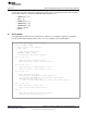
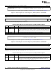
The asynchronous clock configuration register 1 (VCLKACON1) is shown in Figure 18.
Figure 18. Asynchronous Clock Configuration Register 1 (VCLKACON1) Address = 0xFFFFE140
31 27 26 24 23 21 20 19 18 17 16
VCLK4_
Reserved VCLKA4[2:0] Reserved DIV_ VCLKA4S[3:0]
CDDIS
R-0 R/WP-001 R-0 R/WP-1001
15 11 10 8 7 5 4 3 0
VCLK3_
Reserved VCLKA3[2:0] Reserved DIV_ VCLKA3S[3:0]
CDDIS
R-0 R/WP-001 R-0 R/WP-1001
LEGEND: R = Read in all modes; WP = Write in priviledged mode; -n = value after reset
• VCLKA4 is used for the Ethernet controller.
– VCLKA4S field is used to select the clock source for the VCLKA4 domain.
– VCLKA4R field is used to select the divider value to generate the VCLKA4/R frequency.
– VCLKA4_DIV_CDDIS field allows the application to disable the VCLKA4/R signal separately while
the VCLKA4 domain is enabled
• VCLKA3 is not used on the TMS570LS3x microcontrollers.
20
Initialization of Hercules™ ARM
®
Cortex™-R4F Microcontrollers SPNA106– September 2011
Submit Documentation Feedback
Copyright © 2011, Texas Instruments Incorporated