
Specifications


www.ti.com
Standard Initialization Sequence for Hercules Microcontrollers
flashWREG->FPAC2 = 0x000000FF; // PSLEEP = 255 * 16 HCLK cycles
2.10 Clock Domains
There are multiple clock domains on the Hercules microcontrollers to ease the configuration and
controllability of the different modules using these clock domains (see Table 10).
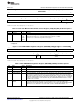
Table 10. Clock Domains on Hercules Microcontrollers
Domain Name Clock Name Comments
GCLK controls all the CPU sub-systems, including the floating point
CPU clock domain GCLK
unit (FPU), and the memory protection unit (MPU)
HCLK shares the same clock source as GCLK, and is always the
System bus clock domain HCLK
same frequency as HCLK.
VCLK_sys is used for the system modules such as VIM, ESM, SYS,
System peripheral clock domain VCLK_sys etc. VCLK_sys is divided down from HCLK by a programmable
divider from 1 to 16.
VCLK is the primary peripheral clock, and is synchronous with
VCLK_sys. VCLK2 is a secondary peripheral clock and is reserved
for use by the enhanced timer module (NHET) and the associated
transfer unit (HTU). VCLK2 is also divided down from HCLK by a
Peripheral clock domains VCLK, VCLK2, VCLK3 programmable divider from 1 to 16. f
HCLK
must be an integer multiple
of f
VCLK2
, f
VCLK2
must be an integer multiple of f
VCLK
. VCLK3 is also
divided down from HCLK by a programmable divider from 1 to 16,
and is used for the Ethernet and EMIF modules on the TMS570LS3x
microcontrollers.
These clock domains are reserved for use by special communication
modules that have strict jitter constraints. The protocols for these
VCLKA1, VCLKA2, and communication modules (e.g., CAN, FlexRay, Ethernet) do not allow
Asynchronous clock domains
VCLKA4 modulated clocks to be used for the baud rate generation. The
asynchronous clocks allow the clock sources for the baud clocks to
be decoupled from the GCLK, HCLK and VCLKx clock domains.
This clock is used for generating the periodic interrupts by the RTI
Real-time Interrupt clock domains RTI1CLK
module.
2.10.1 Mapping Clock Domains to Clock Sources
The system module on the Hercules microcontrollers contains registers that allow the clock domains to be
mapped to any of the available clock sources.
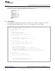
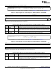
The GCLK, HCLK , VCLKx source register (GHVSRC) is shown in Figure 16 and described in Table 11.
Figure 16. GCLK, HCLK , VCLKx Source Register (GHVSRC) Address = 0xFFFFFF48
31 28 27 24 23 20 19 16
Reserved GHVWAKE[3:0] Reserved HVLPM[3:0]
R-0 R/WP-0000 R-0 R/WP-0000
15 4 3 0
Reserved GHVSRC[3:0]
R-0 R/WP-0000
LEGEND: R = Read in all modes; WP = Write in priviledged mode only; -n = value after reset
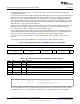
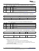
Table 11. GCLK, HCLK , VCLKx Source Register (GHVSRC) Field Descriptions
Bit Field Value Description
31-28 Reserved 0 Reserved
27-24 GHVWAKE Defines the clock source that will be used for the GCLK, HCLK and VCLKx domains when the
microcontroller wakes up from a low power mode. For more details on the low-power modes
supported, see the specific part's technical reference manual.
19
SPNA106– September 2011 Initialization of Hercules™ ARM
®
Cortex™-R4F Microcontrollers
Submit Documentation Feedback
Copyright © 2011, Texas Instruments Incorporated