
Specifications


www.ti.com
Standard Initialization Sequence for Hercules Microcontrollers
Each of the BANKPWRx fields configures the fall-back mode for a single Flash bank. The Hercules
microcontrollers support up to 4 Flash banks.
Configuration of fall-back mode for the Flash banks:
enum flashWPowerModes
{
SYS_SLEEP = 0U, /** flash bank power mode sleep */
SYS_STANDBY = 1U, /** flash bank power mode standby */
SYS_ACTIVE = 3U /** flash bank power mode active */
};
flashWREG->FBFALLBACK = 0x00000000
| (SYS_SLEEP << 6U) // Bank3 falls back to SLEEP
| (SYS_SLEEP << 4U) // Bank2 falls back to SLEEP
| (SYS_SLEEP << 2U) // Bank1 falls back to SLEEP
| SYS_SLEEP; // Bank0 falls back to SLEEP
The above code fragment configures the fall-back mode for each available Flash bank to be the sleep
mode. The application can choose to configure these modes differently as required. The power savings
can be disabled completely by selecting the active state to also be the fall-back power state, which is the
default.
There are a few other registers that control the timing sequence for entry to a fall-back mode and wake up
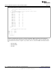
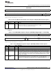
to active mode. The Flash bank access control register is shown in Figure 13 and described in Table 7.
Figure 13. Flash Bank Access Control Register (FBAC) Address = 0xFFF8703C
31 24 23 16
Reserved OTPPROTDIS[7:0]
R-0 R/WP-00000000
15 8 7 0
BAGP[7:0] VREADST[7:0]
R/WP-0 R/WP-00001111
LEGEND: R = Read in all modes; WP = Write in priviledged mode only; -n = value after reset
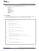
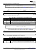
Table 7. Flash Bank Access Control Register (FBAC) Field Descriptions
Bit Field Value Description
31-24 Reserved 0 Reserved
23-16 OTPPROTDIS Not relevant to power modes
15-8 BAGP Configures the Flash banks’ Active Grace Period (AGP). This is the starting count value for a
down-counter. An access to a Flash bank before this counter counts down to 0 causes a reload of
this counter to the configured AGP value. In effect, the AGP delays the Flash banks’ entry into the
selected fall-back mode by 0 to 255 * 16 HCLK cycles. This value must be greater than 1 when the
fall-back mode is not “ACTIVE”.
7-0 VREADST Controls the delay, in terms of HCLK cycles, between the time when the charge pump generates
the required read voltage (VREAD) and the time when the Flash bank starts its own power up
sequence. This time must be at least 100 ns.
NOTE: The Flash banks have hard-coded timings for transitioning from sleep to standby to active
power states. These timings are not configurable by the application.
flashWREG->FMAC = 0x00000003; // Select flash bank3
flashWREG->FBAC |= 0x0000FF00; // Select 255 * 16 HCLK cycles as the bank3 AGP
flashWREG->FMAC = 0x00000002; // Select flash bank2
flashWREG->FBAC |= 0x0000FF00; // Select 255 * 16 HCLK cycles as the bank2 AGP
flashWREG->FMAC = 0x00000001; // Select flash bank1
flashWREG->FBAC |= 0x0000FF00; // Select 255 * 16 HCLK cycles as the bank1 AGP
17
SPNA106– September 2011 Initialization of Hercules™ ARM
®
Cortex™-R4F Microcontrollers
Submit Documentation Feedback
Copyright © 2011, Texas Instruments Incorporated