
Specifications


www.ti.com
Standard Initialization Sequence for Hercules Microcontrollers
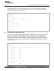
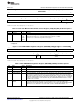
Figure 10. Flash State Machine Write Enable Control Register (FSM_WR_ENA) Address =
0xFFF87288
31 16
Reserved
R-0
15 12 11 8 7 5 4 3 2 1 0
WR
Reserved
ENA
R-0 R/WP-
010
LEGEND: R = Read; WP = Write in priviledge mode; -n = value after reset
Table 5. Flash State Machine Write Enable Control Register (FSM_WR_ENA) Field Descriptions
Bit Field Value Description
31-3 Reserved 0 Reserved
2-0 WR ENA This field enables application to write to the control registers for the Flash module state machine.
101 Privileged mode write access to all other FSM control registers is enabled.
other No write access is allowed to any FSM control register.
value
Once the access to the FSM control registers is enabled, the read access to the flash bank 7 can be
configured.
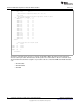
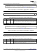
Figure 11. Flash EEPROM Configuration Register (EEPROM_CONFIG) Address = 0xFFF872B8
31 20 19 16
Reserved EWAIT
R-0 R/WP-0001
15 9 8 7 5 4 3 2 1 0
AUTO AUTO
Reserved SUSP START
EN GRACE
R-0 R/WP-0 R/WP-0x02
LEGEND: R = Read; WP = Write in priviledge mode; -n = value after reset
Table 6. Flash EEPROM Configuration Register (EEPROM_CONFIG) Field Descriptions
Bit Field Value Description
31-20 Reserved 0 Reserved
19-16 EWAIT Configures the number of data read wait states for the flash bank 7
15-9 Reserved 0 Reserved
8 AUTO SUSP EN Auto Suspend Enable. This bit, when set, affects the behavior of the Flash module state machine
when the CPU or another bus master accesses the flash bank 7 with an active and suspendable
FSM operation. When this happens, the FSM will automatically be issued a suspend command and
exit from the FSM operation. The bus master access then proceeds. After the access is completed,
the Flash module will wait for a time determined by the AUTOSTART GRACE field before issuing
the FSM resume command.
7-0 AUTOSTART Auto-suspend Start-up Grace Period. The contents of this field determine the duration for which the
GRACE Flash module will wait after the last access to flash bank 7 before ussing the FSM resume
command. The flash module will wait 16 HCLK periods for each count in the AUTOSTART GRACE
field. Each access to flash bank 7 resets the down counter to AUTOSTART GRACE * 16.
15
SPNA106– September 2011 Initialization of Hercules™ ARM
®
Cortex™-R4F Microcontrollers
Submit Documentation Feedback
Copyright © 2011, Texas Instruments Incorporated