
Specifications


Standard Initialization Sequence for Hercules Microcontrollers
www.ti.com
2.8 Configure Flash Access
The Flash memory on the Hercules series microcontrollers is a non-volatile electrically erasable and
programmable memory.
The Hercules microcontrollers contain a digital module that manages all accesses to the Flash memory. A
Flash access can be completed without any wait states required for bus master clock speeds up to 45
MHz. If the bus clock is faster than 45 MHz, then any Flash access requires the appropriate number of
wait states depending on the bus clock speed. The Hercules series microcontrollers support clock speeds
up to 180 MHz. For the actual maximum allowed speed and the number of corresponding address and
data wait states, see the specific part's datasheet.
Suppose that the application requires the microcontroller to run at the maximum supported speed of 180
MHz. This requires 1 address wait state and 3 data wait states for any access to the Flash memory.
These wait states need to be configured in the Flash module registers.
The Flash module also features a pipelined mode of operation. When this mode is enabled, the module
reads 128 bits from the Flash memory and holds them in buffers that the CPU can read from without any
wait state. The CPU can read 32 or 64 bits of instructions or data from the pipeline buffers.
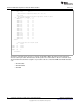
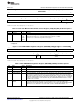
The register inside the Flash module that controls the wait states and the pipeline mode is shown in
Figure 9.
The Flash read control register (FRDCNTL) is shown in Figure 9 and described in Table 4.
Figure 9. Flash Read Control Register (FRDCNTL) Address = 0xFFF87000
31 16
Reserved
R-0
15 12 11 8 7 5 4 3 2 1 0
ASW EN
Reserved RWAIT Reserved Reserved
STEN PIPE
R-0 R/WP-0001 R-0 R/WP-0 R-0 R/WP-0
LEGEND: R = Read; WP = Write in priviledge mode; -n = value after reset
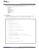
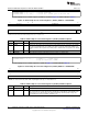
Table 4. Flash Read Control Register (FRDCNTL) Field Descriptions
Bit Field Value Description
31-12 Reserved 0 Reserved
11-8 RWAIT Configures the number of data read wait states
7-5 Reserved 0 Reserved
4 ASWTEN Enables the generation of 1 address wait state. When the address wait state is enabled, the
address bus is latched one cycle before it is decoded for a pipeline hit or miss.
3-1 Reserved 0 Reserved
0 ENPIPE Used to enable or disable the pipeline mode of the Flash module.
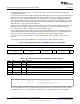
The sequence to configure the wait states and to enable the pipeline mode is as follows.
flashWREG->FRDCNTL = 0x00000000U
| (3U << 8U) // 3 data wait states
| (1U << 4U) // 1 address wait state enabled
| 1U; // Enable pipeline mode
The Hercules MCUs also have a separate flash bank for data storage. This bank can be used to emulate
an EEPROM. Accesses to this flash bank are configured via a separate register in the flash module.
14
Initialization of Hercules™ ARM
®
Cortex™-R4F Microcontrollers SPNA106– September 2011
Submit Documentation Feedback
Copyright © 2011, Texas Instruments Incorporated