
Specifications


www.ti.com
Standard Initialization Sequence for Hercules Microcontrollers
PLL2 is configured using a single PLL Control 3 Register (PLLCTL3) in the System module.
2.8 Enable Clock Sources
2.8.1 Available Clock Sources on Hercules Microcontrollers
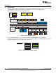
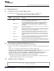
The Hercules microcontrollers support seven different clock sources, as listed in Table 1.
Table 1. Clock Sources on Hercules Microcontrollers
Clock
Source
Number Clock Source Name Description
This is the primary oscillator, typically driven by an external resonator or crystal. This
0 OSCIN is the only available input to the FMPLL and the FMPLL2 macros. The OSCIN
frequency must be between 5 MHz and 20 MHz.
This is the output of the FMPLL, which is generated using the OSCIN as the input
clock. The FMPLL output clock frequency must not exceed the maximum device
1 FMPLL#1 output frequency specified in the device-specific data sheet. The FMPLL features a
modulation mode where a modulation frequency is superimposed on the FMPLL
output signal.
No clock signal is connected to source #2. This clock source must not be enabled or
2 Not implemented
chosen for any clock domain.
External clock input #1. This clock source must only be enabled if there is an actual
3 EXTCLKIN1 external clock source connected to the identified device terminal for EXTCLKIN1. For
more information, see the device-specific data sheet.
This is the low-frequency output of the internal reference oscillator. The LF LPO is
4 LF LPO
typically an 80 KHz signal, and is generally used for low-power mode use cases.
This is the high-frequency output of the internal reference oscillator. The HF LPO is
5 HF LPO typically a 10 MHz signal, and is used as a reference clock for monitoring the main
oscillator.
This is the output of the secondary FMPLL, which is generated using the OSCIN as
6 FMPLL#2 output the input clock. The FMPLL output clock frequency must not exceed the maximum
device frequency specified in the device-specific data sheet.
External clock input #2. This clock source must only be enabled if there is an actual
7 EXTCLKIN2 external clock source connected to the identified device terminal for EXTCLKIN2. For
more information, see the device-specific data sheet.
2.8.2 Control Registers for Enabling and Disabling Clock Sources
There are seven available clock sources on the Hercules microcontrollers:
• Clock sources 0, 4 and 5 are enabled, while clock sources 1, 3, 6 and 7 are disabled upon any system
reset.
• Clock source 2 is not implemented and must not be enabled in the application.
• Each bit of the system module Clock Source Disable Register (CSDIS) controls the clock source of the
same number: bit 0 controls clock source 0, bit 1 controls clock source 1, and so on.
• There are also dedicated Clock Source Disable Set (CSDISSET) and Clock Source Disable Clear
(CSDISCLR) registers to allow the application to avoid using read-modify-write operations.
• Setting any bit commands, the corresponding clock source to be disabled.
– The clock source can only be disabled once there is no clock domain or secondary clock source
(FMPLL, FMPLL#2) using the clock source to be disabled.
2.8.3 Example Clock Source Configuration
systemREG1->CSDISCLR = 0x00000000U
| 0x00000001U // Enable clock source 0
| 0x00000002U // Enable clock source 1
| 0x00000010U // Enable clock source 4
7
SPNA106D–May 2013 Initialization of Hercules™ ARM
®
Cortex™-R4F Microcontrollers
Submit Documentation Feedback
Copyright © 2013, Texas Instruments Incorporated