
Specifications


Standard Initialization Sequence for Hercules Microcontrollers
www.ti.com
2.14 Run Self-Test on the Flash Module SECDED Logic
The Flash module reads the “reset configuration vector” from address 0xF0080140 in the TI OTP region of
Flash bank 0. This is a 64-bit value that is used to configure the device power domains, etc. The Flash
module has built-in SECDED logic to correct any single-bit error in this vector or detect and flag and
double-bit error in this vector. If a double-bit error is detected during this read from the OTP, an ESM
group3 error condition is flagged and the nERROR signal is asserted low. If a single-bit error is detected
during the read from the OTP, this error is corrected by the SECDED logic – no flag is set and no error
signal is sent to the ESM.
There are dedicated locations within the TI OTP sector of Flash bank 0 that are programmed to have
single-bit and double-bit errors. Specifically, a 32-bit or 64-bit read from the address 0xF00803F0 results
in a single-bit error indication, and a 32-bit or 64-bit read from the address 0xF00803F8 results in a
double-bit error indication. These locations can be read by the application to ensure that the Flash
interface module is capable of detecting single-bit and double-bit errors upon reads from the OTP.
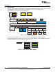
2.15 Clock Domains
All further initializatio steps are now required to be performed at the max operating frequency for the
application. The application must now wait for the PLLs to lock to their target frequencies, and then map
the device clock domains to the desired clock sources. There are multiple clock domains on the Hercules
microcontrollers to ease the configuration and controllability of the different modules using these clock
domains (see Table 2).
Table 2. Clock Domains on Hercules Microcontrollers
Domain Name Clock Name Comments
GCLK controls all the CPU sub-systems, including the floating point
CPU clock domain GCLK
unit (FPU), and the memory protection unit (MPU)
HCLK shares the same clock source as GCLK, and is always the
System bus clock domain HCLK
same frequency as HCLK.
VCLK_sys is used for the system modules such as VIM, ESM, SYS,
System peripheral clock domain VCLK_sys etc. VCLK_sys is divided down from HCLK by a programmable
divider from 1 to 16.
VCLK is the primary peripheral clock, and is synchronous with
VCLK_sys. VCLK2 is a secondary peripheral clock and is reserved
for use by the enhanced timer module (NHET) and the associated
transfer unit (HTU). VCLK2 is also divided down from HCLK by a
Peripheral clock domains VCLK, VCLK2, VCLK3 programmable divider from 1 to 16. f
HCLK
must be an integer multiple
of f
VCLK2
, f
VCLK2
must be an integer multiple of f
VCLK
. VCLK3 is also
divided down from HCLK by a programmable divider from 1 to 16,
and is used for the Ethernet and EMIF modules on the TMS570LS3x
microcontrollers.
These clock domains are reserved for use by special communication
modules that have strict jitter constraints. The protocols for these
VCLKA1, VCLKA2, and communication modules (e.g., CAN, FlexRay, Ethernet) do not allow
Asynchronous clock domains
VCLKA4 modulated clocks to be used for the baud rate generation. The
asynchronous clocks allow the clock sources for the baud clocks to
be decoupled from the GCLK, HCLK and VCLKx clock domains.
This clock is used for generating the periodic interrupts by the RTI
Real-time Interrupt clock domains RTI1CLK
module.
2.15.1 Mapping Clock Domains to Clock Sources
The system module on the Hercules microcontrollers contains registers that allow the clock domains to be
mapped to any of the available clock sources.
The clock source for the GCLK, HCLK , and VCLKx domains is selected by the GCLK, HCLK, VCLK, and
VCLK2 Source Register (GHVSRC).
The clock sources for the VCLKA1 and VCLKA2 domains are selected via the Peripheral Asynchronous
Clock Source Register (VCLKASRC).
10
Initialization of Hercules™ ARM
®
Cortex™-R4F Microcontrollers SPNA106D–May 2013
Submit Documentation Feedback
Copyright © 2013, Texas Instruments Incorporated