
Specifications


www.ti.com
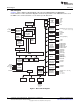
Standard Initialization Sequence for Hercules Microcontrollers
2.11 Configure Flash Bank and Pump Power Modes
The Flash banks and pump used on the TMS570LS043x, TMS570LS033x, and RM42L432 series of
microcontrollers support three different operating modes to optimize power consumption.
• Active mode
– Flash bank sense amplifiers and sense reference are enabled
– All circuits of Flash charge pump are enabled
• Standby mode (only for Flash banks)
– Flash bank sense reference is enabled but sense amplifiers are disabled
• Sleep Mode
– Flash bank sense amplifiers and sense reference are disabled
– All circuits of Flash charge pump are disabled
The Flash banks and charge pump are in the active state by default and after any system reset. The Flash
module allows the application to configure “fall back” power states for the Flash banks and charge pump.
The Flash banks and pump automatically switch the power mode to the selected fall back state when
there is no access to the Flash banks detected within a user-configurable time.
The Flash module also contains special timers to automatically sequence the Flash banks and pump
between the active and the selected fall-back states. A read access to any Flash bank that is in a non-
active power state “wakes up” both the selected bank and the charge pump to active power state.
Programming and erase operations are only allowed on banks in active state.
The Flash Bank Access Control Register (FBAC) controls the Flash banks’ power states.
The Flash Pump Access Control Registers (FPAC1, FPAC2) control the Flash pump's power states.
2.12 Configure Oscillator Monitor
The HF LPO clock source is used as a reference clock for monitoring the main oscillator. A failure is
detected if the oscillator frequency falls outside the range: {f
HFLPO
/ 4, f
HFLPO
*4}.
The HF LPO frequency varies significantly over process corners as well as with changes in the core
supply (V
CC
) and temperature. The Hercules microcontrollers allow the application to trim the HF LPO
such that the application can choose the operating frequency point of the HF LPO. This in turn determines
the valid range of oscillator frequency.
During device test, a trim value is written into the one-time programmable (OTP) section of the Flash
memory, address 0xF008_01B4. Bits 31:16 of this OTP word contain a 16-bit value that may be
programmed into Low Power Oscillator Monitor Control Register (LPOMONCTL) in order to initialize the
trim for HF LPO.
Alternatively, the application can use the dual-clock compare (DCC) module to determine the trim setting
for the HF LPO. The DCC module allows for comparison of two clock frequencies. Once the HF LPO is
determined to be in-range with the initial HFTRIM setting from the OTP, the crystal oscillator may be used
as a reference against which the HF LPO and LF LPO may be further adjusted. For more details, see the
device-specific technical reference manual.
2.13 Run Self-Test on the Flash Module SECDED Logic
The Flash module reads the “reset configuration vector” from address 0xF0080140 in the TI OTP region of
Flash bank 0. This is a 64-bit value that is used to configure the device characteristics at start up. The
Flash module has built-in SECDED logic to correct any single-bit error in this vector or detect and flag any
double-bit error in this vector. If a double-bit error is detected during this read from the OTP, an ESM
group3 error condition is flagged and the nERROR signal is asserted low. If a single-bit error is detected
during the read from the OTP, this error is corrected by the SECDED logic – no flag is set and no error
signal is sent to the ESM.
9
SPNA163–September 2012 Initialization of the TMS570LS043x, TMS570LS033x and RM42L432
Hercules ARM Cortex-R4 Microcontrollers
Submit Documentation Feedback
Copyright © 2012, Texas Instruments Incorporated